Novel homojunction PIN ultraviolet detector
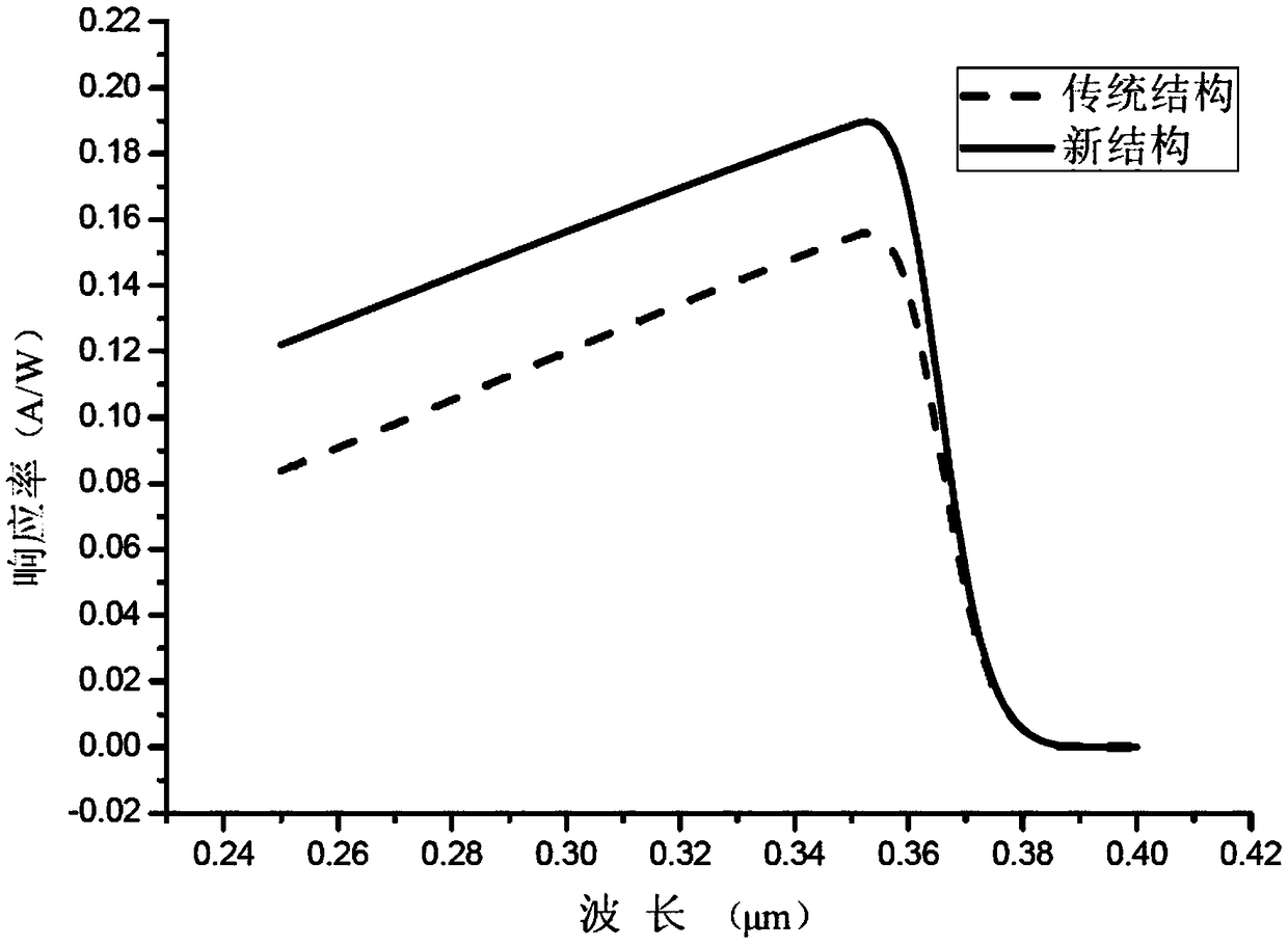
An ultraviolet detector and homojunction technology, applied in semiconductor devices, electrical components, circuits, etc., can solve the problems of increasing dark current, interface polarization, sacrificing short-wave responsivity, etc., to improve spectral responsivity, improve The effect of collection efficiency
- Summary
- Abstract
- Description
- Claims
- Application Information
AI Technical Summary
Problems solved by technology
Method used
Image

Examples
Embodiment 1
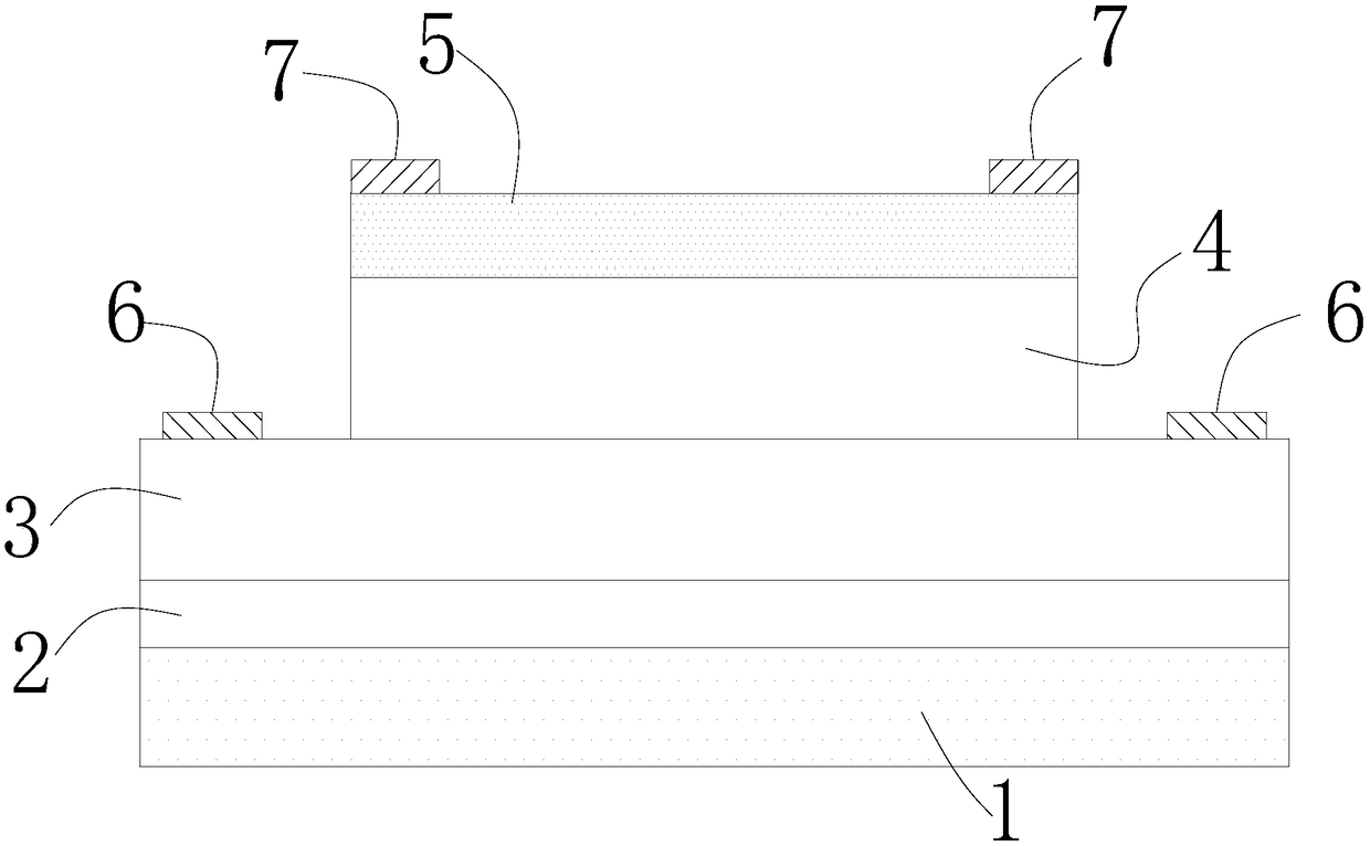
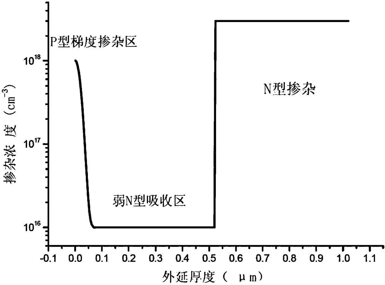
[0021] Such as figure 1 As shown, a new type of homojunction PIN ultraviolet detector, including substrate 1, buffer layer 2, N-type ohmic contact layer 3, absorption layer 4, P-type gradient doping layer 5, N-type ohmic contact electrode 6, P type ohmic contact electrode 7; the buffer layer 2 is arranged on the substrate 1, and the buffer layer 2 is a low-temperature epitaxial AlN material; the N-type ohmic contact layer 3 is arranged on the buffer layer 2, and the N-type ohmic contact layer 3 is a high electron concentration of N-type GaN material; the absorption layer 4 and the N-type ohmic contact electrode 6 are all arranged on the N-type ohmic contact layer 3, the N-type ohmic contact electrode 6 is ring-shaped, and the absorption layer 4 is located on the N-type ohmic contact electrode 6 In the ring, the absorption layer 4 is an unintentionally doped weak N-type GaN material; the P-type gradient doping layer 5 is arranged on the absorption layer 4, and the P-type gradie...
Embodiment 2
[0032] The difference between this embodiment and Embodiment 1 is:
[0033] The buffer layer 2 is a low temperature epitaxial AlN material with a thickness of 200nm.
[0034] The thickness of the N-type ohmic contact layer 3 is 400nm, which is N-type Al with high electron concentration 0.17 Ga 0.83 N material, doping concentration greater than 1×10 18 cm -3 .
[0035] The thickness of the absorbing layer 4 is 400nm, which is unintentionally doped weak N-type Al 0.17 Ga 0.83 N material with a free electron concentration of 1×10 16 cm -3 .
[0036] The P-type gradient doped layer 5 has a thickness of 70nm and is P-type Al 0.17 Ga 0.83 N material.
Embodiment 3
[0038] The difference between this embodiment and embodiment one and two is:
[0039]The buffer layer 2 is a low temperature epitaxial AlN material with a thickness of 300nm.
[0040] The thickness of the N-type ohmic contact layer 3 is 500nm, which is N-type Al with high electron concentration 0.3 Ga 0.7 N material, doping concentration greater than 1×10 18 cm -3 .
[0041] The thickness of the absorbing layer 4 is 500nm, which is unintentionally doped weak N-type Al 0.3 Ga 0.7 N material with a free electron concentration of 1×10 16 cm -3 .
[0042] The P-type gradient doped layer 5 has a thickness of 70nm and is P-type Al 0.3 Ga 0.7 N material.
[0043] The reason for the high responsivity of the detector of the present invention is that when the ultraviolet light is incident from the P-type gradient doped layer 5, due to the Al x Ga 1-x The N material has a large absorption coefficient, and a large amount of ultraviolet rays will be absorbed in the P-type grad...
PUM
| Property | Measurement | Unit |
|---|---|---|
| Thickness | aaaaa | aaaaa |
| Thickness | aaaaa | aaaaa |
| Doping concentration | aaaaa | aaaaa |
Abstract
Description
Claims
Application Information