Supercharge Your Innovation With Domain-Expert AI Agents!

Black silicon nano-pin photodetector structure and its preparation method

A photodetector and nanostructure technology, applied in circuits, electrical components, semiconductor devices, etc., can solve problems such as restricting national defense capabilities, increasing the economic burden of ordinary people, and restricting exploration capabilities.

Active Publication Date: 2020-07-07
INST OF MICROELECTRONICS CHINESE ACAD OF SCI
View PDF7 Cites 0 Cited by
  • Summary
  • Abstract
  • Description
  • Claims
  • Application Information

AI Technical Summary

Problems solved by technology

However, my country's semiconductor detectors mainly rely on imports. Whether it is high-end or low-end products, it seriously restricts my country's national defense capabilities in the military, limits my country's ability to explore the frontiers of science and technology in terms of high-tech development, and greatly increases the number of ordinary people in terms of civilian use. economic burden

Method used


Image

  • Black silicon nano-pin photodetector structure and its preparation method
  • Black silicon nano-pin photodetector structure and its preparation method

Examples


preparation example Construction

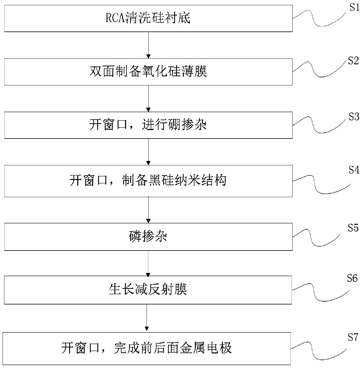
[0034] The disclosure also provides a method for preparing a black silicon nano-PIN photodetector structure, such as figure 2 Shown, the preparation method of described its black silicon nanometer PIN photodetector structure comprises the following steps:

[0035] S1, cleaning the P-type crystalline silicon substrate with standard RCA;

[0036] S2, preparing a silicon oxide film on both sides of the cleaned silicon substrate;

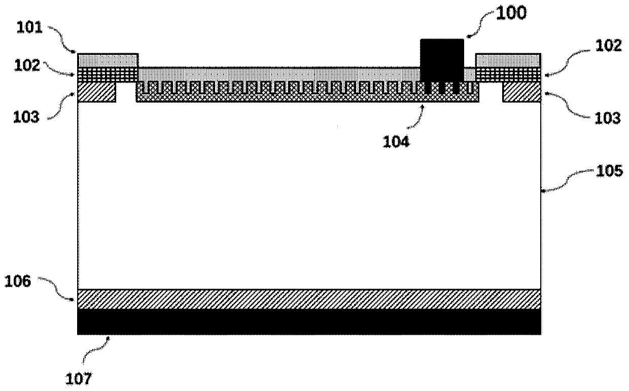
[0037] S3, opening a boron diffusion window on the front surface and back surface of the silicon substrate covered with silicon oxide film, and performing boron doping to form a front surface protection ring (that is, a front surface boron-doped protection ring) and a back surface P+ heavily doped region;

[0038] S4, opening a phosphorus diffusion window on the front surface of the boron-doped silicon substrate, and preparing a black silicon nanostructure;

[0039] S5, performing phosphorus doping in the black silicon nanostructure region to form a...


PUM

PropertyMeasurementUnit
diameteraaaaaaaaaa
depthaaaaaaaaaa
thicknessaaaaaaaaaa

Abstract

The invention provides a structure and a preparation method of a black silicon nanometer PIN photoelectric detector, wherein the structure of the black silicon nanometer PIN photoelectric detector comprises a front surface metal electrode, a front surface anti-reflection film, a front surface silicon oxide film, a front surface N-type heavily doped zone, a P-type crystal silicon substrate, a backsurface P-type heavily doped zone, and a back surface metal electrode from the top to bottom in sequence, wherein the black silicon nanometer structure is adopted by the front surface N-type heavily doped zone. By virtue of the structure and the preparation method of the black silicon nanometer PIN photoelectric detector, the breakdown voltage of the detector is greatly improved and acquisition ofhigher spectral response can be facilitated.

Description

technical field [0001] The disclosure relates to the technical field of silicon-based photodetectors, in particular to a black silicon nano-PIN photodetector structure and a preparation method thereof. Background technique [0002] Semiconductor detectors play an important and irreplaceable role in both military and civilian use. The products are used in a large amount and have a wide range. Taking silicon-based PIN structure photodetectors as an example, they are widely used in security inspection equipment in Beijing subways. Imaging systems rely on silicon-based PIN photodetectors, as well as remote controls such as refrigerators and TVs in homes, imaging systems in CT equipment in hospitals, and so on. However, my country's semiconductor detectors mainly rely on imports. Whether it is high-end or low-end products, it seriously restricts my country's national defense capabilities in the military, limits my country's ability to explore the frontiers of science and technolo...

Claims


Application Information

Patent Timeline
Patent Type & Authority Patents(China)
IPC IPC(8): H01L31/105H01L31/0236H01L31/0352H01L31/18
CPCH01L31/02363H01L31/035272H01L31/105H01L31/1804Y02P70/50
Inventor 陶科贾锐孙恒超戴小宛姜帅周颖
Owner INST OF MICROELECTRONICS CHINESE ACAD OF SCI
Features
  • R&D
  • Intellectual Property
  • Life Sciences
  • Materials
  • Tech Scout
  • Unparalleled Data Quality
  • Higher Quality Content
  • 60% Fewer Hallucinations
Learn More