Filtering method

A filter and square hole technology, which is applied in the field of micro-nano optoelectronics, can solve the problems of low transmittance and large size of waveguide filters, and achieve the effects of high light transmittance, small size, and easy integration

Active Publication Date: 2018-07-31
安徽翰邦科技咨询有限公司
View PDF6 Cites 2 Cited by
  • Summary
  • Abstract
  • Description
  • Claims
  • Application Information

AI Technical Summary

Problems solved by technology

[0009] The present invention needs to solve the problems of low transmittance and large size of traditional waveguide filters, and provides a filtering method

Method used


Image

  • Filtering method
  • Filtering method
  • Filtering method

Examples


Embodiment Construction

[0029] The present invention will be further described below in conjunction with embodiment.

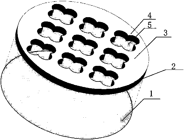
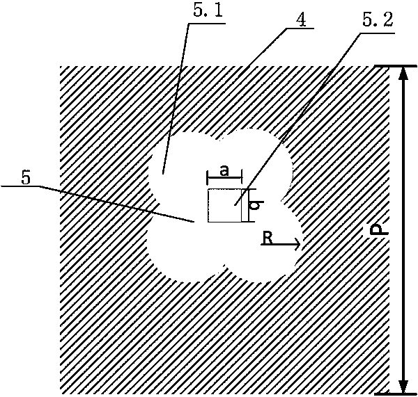
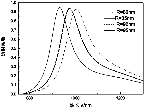
[0030] A plasmonic waveguide filter with strong transmission characteristics, including an optical fiber substrate 1, a metal film 2 and a dielectric layer 3, the optical fiber substrate 1 is arranged directly under the metal film 2, and the dielectric layer 3 is laid on the metal film 2 On the upper surface, the metal film 2 is uniformly arranged with N unit hole array structures 4; the thickness of the metal film 2 is 60nm, and the metal film 2 can also have other thicknesses. Optionally, the thickness of the metal film 2 is not limited to 60nm, and the material of the metal film can be gold or silver. The number N of the unit hole array structures 4 on the metal film 2 is generally a positive integer ranging from 25 to 60, and users can choose other numbers according to their needs. figure 1 Only 9 unit hole array structures 4 are drawn in the figure; the unit hole array structur...


PUM


Abstract

The invention provides a filtering method, and belongs to the field of micro-nano photoelectron. The method comprises the steps that the plane wave is vertically and downwardly incident from the uppersurface of a dielectric layer (3) and emergent from the lower surface of a metal film (2) or the plane wave is vertically and upwardly incident from the lower surface of the metal film (2) and transmits through the upper surface of the dielectric layer (3); and when the plane wave beam is vertically incident into one of the surfaces of the metal film (2), the long range surface plasmons producedby the adjacent circular holes and the local area surface plasmons produced by the square holes are inter-coupled through the nano narrow gap so as to form an electromagnetic field. According to the method, light transmission can be greatly enhanced and the method has great spectral characteristics.

Description

[0001] This application is a divisional application of the invention patent application "A Plasmon Waveguide Filter with Strong Transmission Characteristics". [0002] The original filing date: 2016-04-29. [0003] Original application number: 2016102810356. [0004] The name of the original invention: a plasmonic waveguide filter with strong transmission characteristics. technical field [0005] The invention relates to the field of micro-nano optoelectronics, in particular to a filtering method. Background technique [0006] Surface plasmons are a special electromagnetic wave mode that exists on the surface of metal electrolytes. It is produced by the collective oscillation of free electrons on the metal surface under the excitation of incident light. This special electromagnetic wave propagates along the direction of the metal surface and decays exponentially in the direction perpendicular to the metal surface. Due to its unique surface wave characteristics, it can con...

Claims


Application Information

Patent Timeline
Patent Type & Authority Applications(China)
IPC IPC(8): G02B5/00G02B5/20G02B6/02
CPCG02B5/008G02B5/20G02B6/02052G02B6/02295G02B6/262
Inventor 不公告发明人
Owner 安徽翰邦科技咨询有限公司
Why Eureka
Try Eureka