
Charge generation layer, electroluminescent device and preparation method thereof

A technology of electroluminescent devices and charge generation layers, which is applied in the fields of electric solid devices, semiconductor/solid device manufacturing, electrical components, etc., which can solve the problem of changing the electrical characteristics of organic layers, reducing the light transmittance of devices, and not being easy to large-scale and other issues to achieve the effect of improving performance, improving luminous efficiency and device life, and avoiding damage

Active Publication Date: 2018-07-31
GUANGDONG JUHUA PRINTING DISPLAY TECH CO LTD
View PDF7 Cites 0 Cited by
  • Summary
  • Abstract
  • Description
  • Claims
  • Application Information

AI Technical Summary

Problems solved by technology

[0004] At present, the charge generation layers of stacked organic light-emitting diodes reported are all formed based on evaporation or sputtering film formation technology, and the materials used are generally metal materials. On the one hand, the preparation process is complicated and it is not easy to achieve large-area; on the other hand, On the one hand, high temperature is required for evaporating or sputtering the intermediate electrode (charge generation layer), which is easy to damage the organic layer, resulting in changes in the electrical properties of the organic layer, affecting device performance, and the intermediate metal electrode will reduce the light transmittance of the device , can form a strong microcavity effect, resulting in color change and spatial color change with different viewing angles

Method used


Image

  • Charge generation layer, electroluminescent device and preparation method thereof

Examples


Embodiment 1

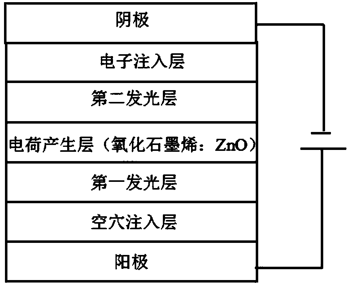
[0074] This embodiment provides an electroluminescent device, the preparation method of which comprises the following steps:

[0075] Cleaning the substrate: The glass substrate with 150nm ITO is ultrasonically cleaned in five steps of deionized water, acetone, lotion, deionized water and isopropanol, each step is 10-15 minutes, after cleaning, it is dried in a vacuum oven spare;

[0076] Plasma treatment substrate: The dried ITO is subjected to oxygen plasma treatment for 4 minutes, and the ITO layer after plasma treatment is used as the anode layer;

[0077] Preparation of hole injection layer: Within half an hour after Plasma treatment, spin-coat PEODT:PSS solution on the surface of the anode layer, and then heat in air at 120°C for 20 minutes to form a 40nm-thick hole injection layer;

[0078] Preparation of the first light-emitting layer: transfer the dried ITO spin-coated with PEDOT:PSS into the glove box, spin-coat the xylene solution of P-PPV on the surface of the hol...

Embodiment 2

[0085] This embodiment provides an electroluminescent device, the preparation method of which is basically the same as that of Embodiment 1, except that the mass ratio of graphene oxide and nano zinc oxide is 0.8:1.

Embodiment 3

[0087] This embodiment provides an electroluminescent device, the preparation method of which is basically the same as that of Embodiment 1, except that the mass ratio of graphene oxide and nano zinc oxide is 1.2:1.

[0088] In the electroluminescence device prepared in the above embodiments, individual light-emitting units are connected in series to form a complete device, which can realize the superposition of current efficiency and prolong the service life of the device. In addition, the charge generation layer is prepared by solution processing, which can effectively avoid damage to the organic light-emitting layer caused by high temperature during evaporation or sputtering of the intermediate electrode. Simultaneously, since the organic light-emitting layer is generally dissolved with a weak polar solvent (such as xylene, toluene), the charge generation layer of the present invention is dissolved with a strong polar solvent, which can effectively prevent the charge generat...


PUM


Abstract

The invention relates to a solution-processable charge generation layer, an organic electroluminescent device and a preparation method thereof. The charge generation layer is prepared by a mixture, wherein the mixture is formed by dispersing a component which at least comprises an N-type semiconductor material and a P-type semiconductor material into a strongly polar solvent, and the energy leveldifference between the highest occupied molecular orbital of the P-type semiconductor material and the lowest unoccupied molecular orbital of the N-type semiconductor material is less than 0.6eV. Thecharge generation layer can be prepared in an all-solution processing mode, the preparation condition is mild, damages imposed on an organic light emitting layer by a high temperature during evaporation or sputtering of an intermediate electrode can be effectively avoided, the processibility of the device is ensured, and thus the performance of the device is improved. The charge generation layer is further prepared into an electroluminescent device, independent light emitting units are connected in series to form a complete device, and the light emitting efficiency and the device life of the device are greatly improved.

Description

technical field [0001] The invention relates to the field of organic light-emitting diodes, in particular to a solution-processable charge generation layer, an electroluminescence device and a preparation method thereof. Background technique [0002] Organic light-emitting diodes have broad application prospects in full-color display, backlight and solid-state lighting, and have attracted widespread attention. Solution-processed organic light-emitting diodes based on inkjet printing technology are more popular due to their advantages of low cost and easy realization of large-area production, but the device performance (low current efficiency, etc.) Therefore, solution-type organic light-emitting diodes need to optimize the device structure to greatly improve the overall performance of the device. [0003] Conventional OLEDs contain only one light-emitting unit (single-layer device). In 2003, Kido et al. proposed the concept of stacked organic light-emitting diodes, that is...

Claims


Application Information

Patent Timeline
Patent Type & Authority Applications(China)
IPC IPC(8): H01L51/50H01L51/56
CPCH10K50/131H10K50/17H10K71/00
Inventor 余磊
Owner GUANGDONG JUHUA PRINTING DISPLAY TECH CO LTD
Learn More