
LED chip and manufacturing method thereof

A technology of LED chips and manufacturing methods, which is applied in the direction of electrical components, circuits, semiconductor devices, etc., can solve the problems of high cost and increase the amount of light output, and achieve the effects of high cost, reduced manufacturing cost, and high adhesion

Inactive Publication Date: 2018-08-03
ENRAYTEK OPTOELECTRONICS
View PDF0 Cites 2 Cited by
  • Summary
  • Abstract
  • Description
  • Claims
  • Application Information

AI Technical Summary

Problems solved by technology

[0006] The reflective layer used in both flip-chip and vertical LED chips relies on the high reflectivity of Ag and other metals to directional reflect the light emitted by the quantum well layer to the bottom of the chip to increase the amount of light; the Ag layer is then sequentially Coated with TiW (titanium tungsten) layer and Pt (platinum gold) layer to prevent Ag diffusion, but the cost of using Pt is higher

Method used


Image

  • LED chip and manufacturing method thereof
  • LED chip and manufacturing method thereof
  • LED chip and manufacturing method thereof

Examples


Embodiment Construction

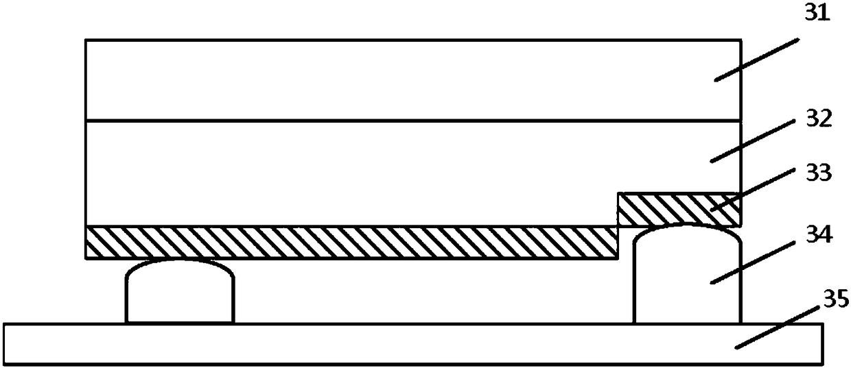
[0048] The invention provides an LED chip and a manufacturing method thereof. The structure of Ag-TiW-Ti (silver-titanium tungsten-titanium) is used in the reflective layer of the LED chip, and the protection of the silver layer is realized by two metals, titanium tungsten and titanium. Prevents silver leaching and flow, and highly adherent metal enables adhesion to subsequent films. The reflective layer metal structure described in the present invention is suitable for LED chips with flip-chip structure or vertical structure.

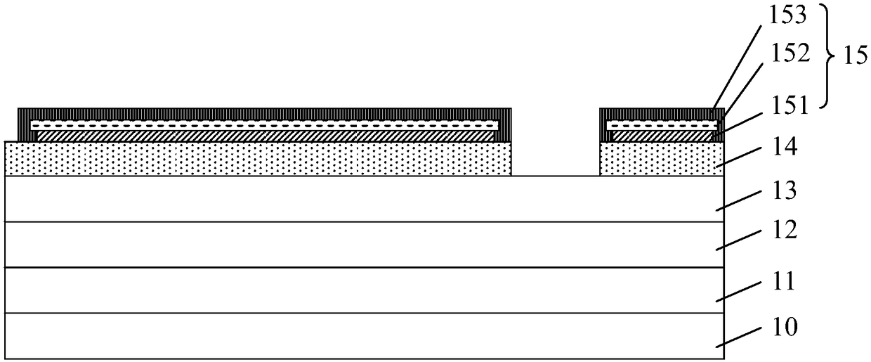
[0049] like Figure 3 ~ Figure 6As shown, the LED chip with flip-chip structure and its manufacturing method include the following processes:

[0050] like image 3 As shown, a front-end structure is provided, including a sapphire substrate 10, and an N-GaN layer 11, a quantum well layer 12, and a P- GaN layer 13.

[0051] Form the ohmic contact layer 14 on the surface of the front-end structure, and pattern it to expose the P-GaN layer 13; the mat...


PUM

PropertyMeasurementUnit
Thicknessaaaaaaaaaa
Thicknessaaaaaaaaaa

Abstract

The invention relates to an LED chip and a manufacturing method thereof. According to the LED chip and manufacturing method thereof, titanium tungsten and titanium metal are additionally arranged on ahigh-reflectivity silver layer, so as to prevent silver diffusion and increase the adhesiveness of a subsequent film layer, thus a reflective layer thin film has high stability and high adhesion, andthe manufacturing cost can be effectively reduced. The manufacturing method is applicable to the LED chip of a flip-chip structure or vertical structure.

Description

technical field [0001] The invention relates to the technical field of semiconductors, in particular to an LED chip and a manufacturing method thereof. Background technique [0002] The mainstream chip structures in the LED industry are generally divided into three types: front-mount, flip-chip, and vertical. Among them, flip-chip and vertical chips have attracted more attention because of their high performance compared with formal-mount products. [0003] For traditional front-mounted LED chips, P-type GaN is difficult to dope, resulting in low hole carrier concentration and difficulty in growing thick, resulting in difficult diffusion of current. At present, the method of preparing ultra-thin metal film or ITO film on the surface of P-type GaN is generally used to achieve The current has to spread evenly. However, the metal thin film electrode layer has to absorb part of the light to reduce the light extraction efficiency, and if the thickness is reduced, it will in turn...

Claims


Application Information

Patent Timeline
IPC IPC(8): H01L33/40H01L33/00
CPCH01L33/405H01L33/007
Inventor 王亚洲邵明镜陈党盛
Owner ENRAYTEK OPTOELECTRONICS
Features
  • Generate Ideas
  • Intellectual Property
  • Life Sciences
  • Materials
  • Tech Scout
  • Unparalleled Data Quality
  • Higher Quality Content
  • 60% Fewer Hallucinations
Learn More