Electroluminescent device

An electroluminescent device and device technology, applied in the direction of electric solid-state devices, electrical components, semiconductor devices, etc., can solve the problems of low luminous efficiency and achieve the effect of improving luminous efficiency

Active Publication Date: 2018-08-03
BEIJING VISIONOX TECH
View PDF12 Cites 9 Cited by
  • Summary
  • Abstract
  • Description
  • Claims
  • Application Information

AI Technical Summary

Problems solved by technology

[0007] The embodiment of the present application provides an electroluminescent device, which is used to solve the problem of low luminous efficiency of existing organic / inorganic composite electroluminescent devices

Method used


Image

  • Electroluminescent device
  • Electroluminescent device
  • Electroluminescent device

Examples


Embodiment 1

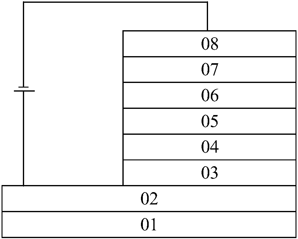
[0041] figure 1 It is a schematic structural diagram of an electroluminescent device provided in Example 1 of the present application. see figure 1 , the electroluminescent device may specifically include: a substrate 01, an anode 02, a hole transport layer 03, an inorganic light-emitting layer 06, an electron transport layer 07, and a cathode 08, and further includes:

[0042] An electron donor layer 04 located between the phosphorescent layer 06 and the hole transport layer 03 and an electron acceptor layer 05 located between the electron donor layer 04 and the phosphorescent layer 06;

[0043] The organic electron donor molecules carried by the electron donor layer 04 and the organic electron acceptor molecules carried by the electron acceptor layer 05 form an interface exciplex.

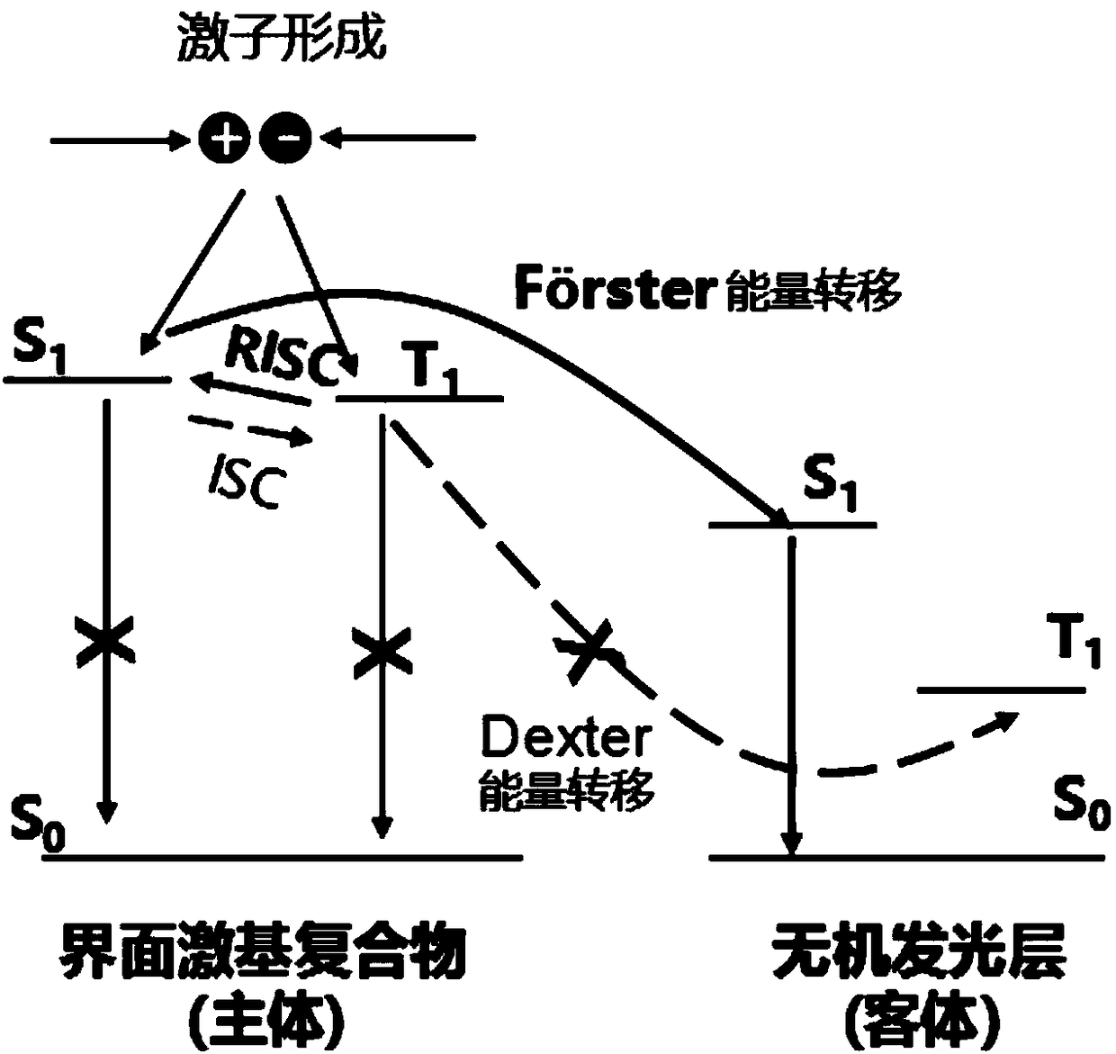
[0044] It should be noted that the interface excitons corresponding to exciplexes are also called electron-hole pairs, which consist of one electron and one hole. Among them, electrons are inj...

Embodiment 2

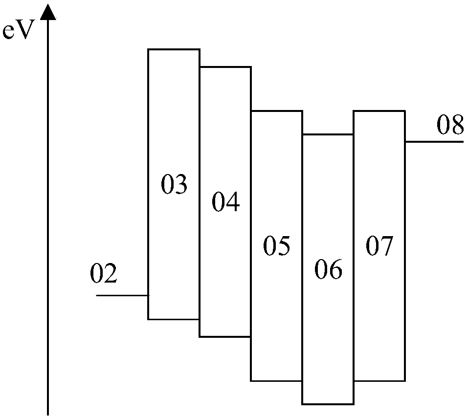
[0067] Figure 4a-Figure 4c For a schematic diagram of the energy level structure of an electroluminescent device provided in Example 2 of the present application, see Figure 4a-Figure 4c , on the basis of the electroluminescent device provided in Example 1, this embodiment provides three electroluminescent devices with optimized structures, specifically as follows:

[0068] The first optimization structure: see Figure 4a ,exist figure 1 On the basis of the electroluminescence device shown, it further includes: an electron blocking layer 09 .

[0069] The electron blocking layer 09 is located between the hole transport layer 03 and the electron donor layer 04 .

[0070] The second optimization structure: see Figure 4b ,exist figure 1 On the basis of the shown electroluminescent device, it further includes: a hole blocking layer 10 .

[0071] The hole blocking layer 10 is located between the phosphorescent layer 06 and the electron transport layer 07 .

[0072] The th...

Embodiment 3

[0078] Figure 5 For a structural schematic diagram of an electroluminescent device provided in Example 3 of the present application, see Figure 5 , the electroluminescent device may specifically include in turn: a substrate 51, a cathode 58, an electron transport layer 57, an inorganic light-emitting layer 56, an electron acceptor layer 55, an electron donor layer 54, a hole transport layer 53, and an anode 52, wherein:

[0079] The organic electron donor molecules carried by the electron donor layer 55 and the organic electron acceptor molecules carried by the electron acceptor layer 54 form an interface exciplex.

[0080] Wherein, the material of the electron transport layer 57 can be an organic electron transport material, zinc oxide ZnO, titanium oxide TiO 2 , one or more of nickel oxide NiO.

[0081] It should be noted that, compared with conventional devices, the inverted structure device used in this embodiment, on the one hand, has changed the positions of cathode ...


PUM


Abstract

The invention discloses an electroluminescent device which comprises a substrate, an anode, a cavity transmission layer, an electron donor layer, an electron acceptor layer, an inorganic luminescent layer, an electron transmission layer and a cathode successively, and an organic electron donor molecule carried by the electron donor layer and an organic electron acceptor molecule carried by the electron acceptor layer form an interface exciplex. The electron donor layer and electron acceptor layer are additionally arranged to form the interface exciplex as the main body, triplet-state excitonsof the interface exciplex can be converted into singlet excitons via reverse intersystem crossing, and the singlet excitons are sensitized into the inorganic luminescent layer as an object via a fluorescence resonance energy transduction manner to emit light, and the light emitting efficiency can be improved.

Description

technical field [0001] The present application relates to the field of display technology, in particular to an electroluminescent device. Background technique [0002] Electroluminescence, also known as electric field luminescence, is an electric field generated by the voltage applied to the two electrodes, and the electrons excited by the electric field hit the luminescent center, which causes the transition, change, and recombination of electrons between energy levels to cause luminescence. a physical phenomenon. [0003] At present, the light-emitting mechanism of inorganic materials in organic / inorganic composite electroluminescent devices can be divided into direct injection type and energy transfer type, among which: [0004] In injection-type light-emitting devices, on the one hand, the highest occupied molecular orbital (HOMO) energy level of the inorganic light-emitting layer is too deep (usually exceeding -6.5eV), which does not match the HOMO energy level (-5~-6e...

Claims


Application Information

Patent Timeline
Patent Type & Authority Applications(China)
IPC IPC(8): H01L51/50
CPCH10K50/11H10K2101/40H10K2102/00
Inventor 黄根茂黄秀颀闵超袁波刘胜芳徐琳李雪原
Owner BEIJING VISIONOX TECH
Why Eureka
Try Eureka