Supercharge Your Innovation With Domain-Expert AI Agents!

Silicon thin film material stress detection system

A technology of material stress and detection system, which is applied in the measurement of force, force/torque/power measuring instrument, measuring device, etc. by measuring the change of optical properties of the material when it is stressed, can solve the problem of inability to measure the stress of the sample and the inability to silicon Sample measurement and other issues, to achieve the effect of accurate testing and simple operation

Inactive Publication Date: 2018-08-10
INNER MONGOLIA UNIV OF TECH
View PDF5 Cites 3 Cited by
  • Summary
  • Abstract
  • Description
  • Claims
  • Application Information

AI Technical Summary

Problems solved by technology

However, this method can only measure the stress generated by the external force on the sample, and cannot measure the stress existing in the sample itself.
[0006] The surface second harmonic method is based on the second harmonic phenomenon of the silicon surface (that is, the second harmonic of the silicon surface is generated by the stress existing in the silicon sample breaking its inversion symmetry, and the stress of the sample itself can be offset by the external stress. Make the measured second harmonic disappear) to measure the stress on the surface of the silicon sample, but this method can only measure the depth of about 100nm on the silicon surface, and cannot conduct a comprehensive measurement of the entire silicon sample

Method used


Image

  • Silicon thin film material stress detection system
  • Silicon thin film material stress detection system
  • Silicon thin film material stress detection system

Examples


Embodiment Construction

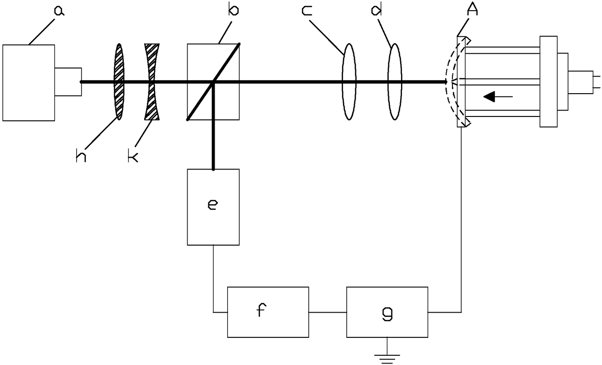
[0025] The embodiments of the present invention will be described in detail below with reference to the accompanying drawings, but the present invention can be implemented in many different ways defined and covered by the claims.

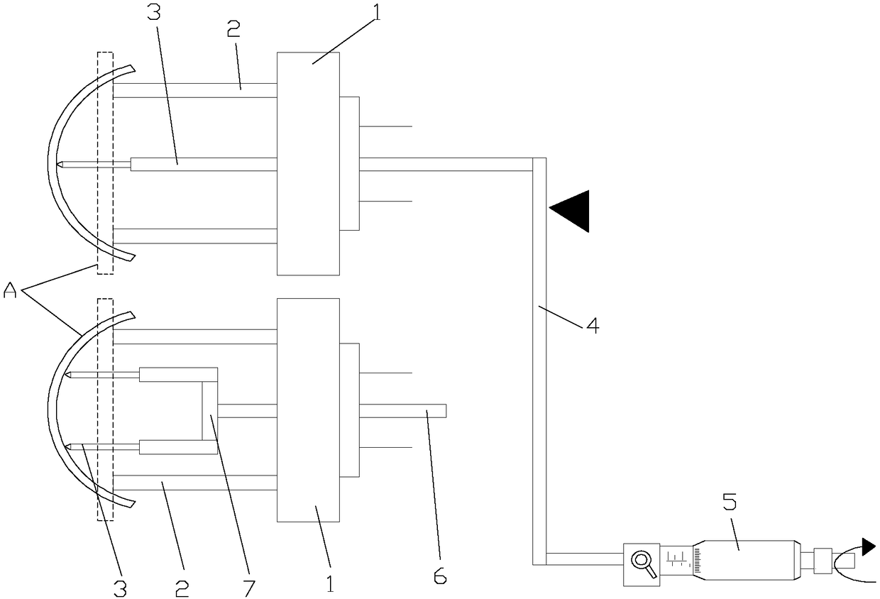
[0026] Such as figure 1 and figure 2 As shown, a kind of silicon film material stress detection system provided in this embodiment, it comprises:

[0027] A laser a is used as a laser beam emitting device. As a preferred solution, a solid-state laser with continuously adjustable output optical power can be used; according to the detection requirements, the wavelength of the laser a emitted beam is 1550nm, and the output optical power is 0-3W Adjustable within the range and the spot is a circular spot with a diameter within 0.8mm;

[0028] Polarizing beam splitter b, which is arranged on the light output side of laser a along the Z-axis direction, is mainly used to convert the output beam of laser a into linearly polarized light that vibrates vert...


PUM

PropertyMeasurementUnit
electrical resistivityaaaaaaaaaa

Abstract

The invention relates to the technical field of photoelectric detection and especially relates to a silicon thin film material stress detection system. The system comprises a laser, a polarization beam splitter, a quarter wave plate, a half wave plate and a stress application device, which are arranged in sequence in the Z-axis direction. The system also comprises a reflected light detector for receiving reflected light of the polarization beam splitter and converting the reflected light into an electrical signal, an analog phase-locked amplifier connected with the reflected light detector, and a low-frequency signal generator for applying a modulated field to a sample and meanwhile, is connected with the analog phase-locked amplifier. The stress application device comprises a positioningdisc, a metal fixation rod and a stress application rod. The system realizes the purpose of comprehensive detection of silicon material stress through a three-point method or a four-point method and the like based on the characteristic that stress can enable the silicon material to have a linear electro-optic effect; and the system is simple in structure, and can carry out comprehensive and accurate stress detection on the silicon film material without requiring detection personnel to have rich background knowledge.

Description

technical field [0001] The invention relates to the technical field of photoelectric detection, in particular to a silicon thin film material stress detection system. Background technique [0002] As we all know, silicon material, as a semiconductor material with low price and mature technology, is not only the first choice material for integrated circuits, but also widely used in all aspects of electronic products and has more and more advantages in the field of silicon-based optoelectronics. application value. However, due to the limitation of production and processing technology level (such as quenching technology level) and the influence of factors such as its contact with other materials or the existence of periodic natural termination characteristics at its own edge, residual stress will be generated in silicon materials, and the residual stress The production will greatly affect the performance and quality of silicon materials and their application devices. Therefor...

Claims


Application Information

Patent Timeline
Patent Type & Authority Applications(China)
IPC IPC(8): G01L5/00G01L1/24
CPCG01L1/24G01L5/0047
Inventor 朱景程孟建英蒋丹蕊刘日王景峰宋智青
Owner INNER MONGOLIA UNIV OF TECH
Features
  • R&D
  • Intellectual Property
  • Life Sciences
  • Materials
  • Tech Scout
  • Unparalleled Data Quality
  • Higher Quality Content
  • 60% Fewer Hallucinations
Learn More