Chip package structure and chip package method

A chip packaging structure and chip packaging technology, applied in electrical components, electrical solid devices, circuits, etc., can solve the problems of low production efficiency and complex chip packaging structure, and achieve high production efficiency, easy industrial preparation, and increased distance. Effect

Inactive Publication Date: 2018-08-10
NAT CENT FOR ADVANCED PACKAGING
View PDF3 Cites 0 Cited by
  • Summary
  • Abstract
  • Description
  • Claims
  • Application Information

AI Technical Summary

Problems solved by technology

[0005] The technical problem to be solved by the present invention is to overcome the defects of complex chip packaging structure and low production efficiency in the prior art

Method used


Image

  • Chip package structure and chip package method
  • Chip package structure and chip package method
  • Chip package structure and chip package method

Examples


Embodiment 1

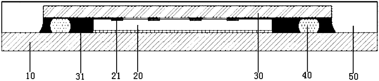
[0044] An embodiment of the present invention provides a chip packaging structure, such as figure 1 As shown, it includes a substrate 10 , and a gold back chip 20 and an interposer 30 sequentially disposed on the substrate 10 . Wherein, the first surface of the gold-backed chip 20 (ie, the gold-backed surface) is electrically connected to the substrate 10 , and the second surface of the gold-backed chip 20 (ie, the front surface, the surface opposite to the gold-backed surface) is electrically connected to the adapter plate 30 .

[0045] By mounting the back gold chip 20 on the adapter plate 30, that is, the back gold chip 20 is arranged between the substrate 10 and the adapter plate 30 and the back gold surface is electrically connected to the substrate 10, and the front side is facing upward, the standard The flip-chip process realizes chip packaging, and the packaging structure is simple, easy for industrial preparation; the preparation efficiency is high, and it is suitabl...

Embodiment 2

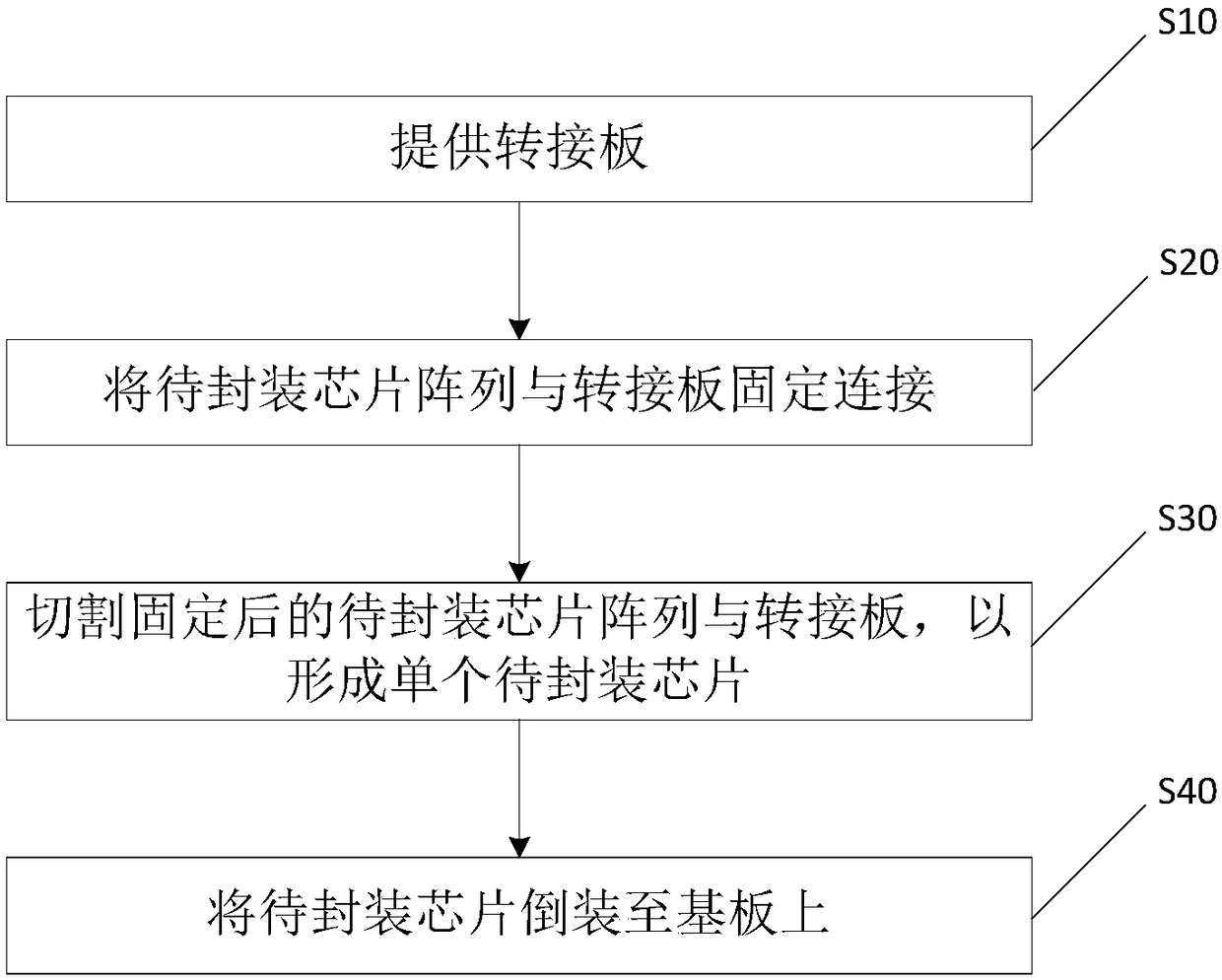
[0057] An embodiment of the present invention provides a chip packaging method, such as figure 2 As shown, the method includes the following steps:

[0058] Step S10, providing an adapter board.

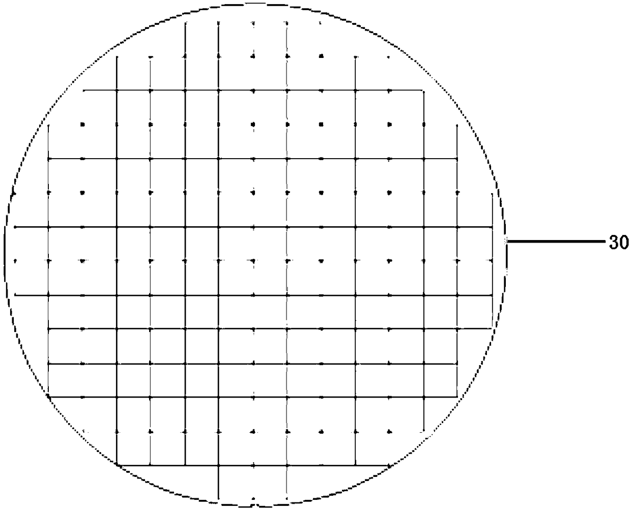
[0059] The adapter plate 30 is a silicon adapter plate, Figure 3a A top view of the interposer 30 is shown, and the subsequent processing technology of the interposer 30 can be realized through a wafer process. Specifically, the following steps are included:

[0060] In step S11 , a redistribution layer 31 is formed on the surface of the interposer board 30 .

[0061] The fabrication of the redistribution layer 31 on the surface of the adapter board 30 is realized through the wafer process, which corresponds to the IO pins on the surface of the chip 20 to be packaged one by one. design.

[0062] Wherein, forming the redistribution layer 31 on the surface of the interposer board 30 may specifically include:

[0063] A metal layer is formed on the surface of the interposer 30, ...


PUM


Abstract

The invention relates to the field of semiconductor package technology, and provides a chip package structure and a chip package method. The chip package structure comprises: a substrate; and a to-be-packaged chip and an adapter plate, which are arranged on the substrate in sequence, wherein a first surface of the to-be-packaged chip is electrically connected to the substrate, and a second surfaceopposite to the first surface is electrically connected to the adapter plate. By fitting the to-be-packaged chip on the adapter plate, that is, the to-be-packaged chip is arranged between the substrate and the adapter plate, the chip package can be implemented by using a standard upside-down assembly process, and the package structure is simple and easy to be industrially prepared; and the preparation efficiency is high, and the chip package structure is suitable for mass production.

Description

technical field [0001] The invention relates to the technical field of semiconductor packaging, in particular to a chip packaging structure and a chip packaging method. Background technique [0002] The reason why flip-chip (Flip-Chip, referred to as FC) is called "flip-chip" is relative to the traditional wire bonding (Wire Bonding) connection method and the process after ball planting. The electrical side of the traditional chip connected to the substrate by wire bonding faces up, while the electrical side of the flip chip faces down, which is equivalent to turning the former upside down, so it is called a flip chip. Flip-chip has smaller dimensions, smaller ball diameter and pitch, and has unique advantages in terms of product cost, performance, and high-density packaging. Therefore, flip chips have been widely used in miniaturized, high-density, high-performance packaged products in recent years. [0003] At present, chip flip-chip is realized mainly because the incomi...

Claims


Application Information

Patent Timeline
Patent Type & Authority Applications(China)
IPC IPC(8): H01L23/31H01L23/498H01L23/49H01L21/56
CPCH01L21/56H01L23/31H01L23/49H01L23/498
Inventor 周鸣昊孙亚楠
Owner NAT CENT FOR ADVANCED PACKAGING
Why Eureka
Try Eureka