Flexible array substrate, preparation method thereof and flexible display panel

A flexible array and substrate technology, applied in electrical components, electrical solid devices, circuits, etc., can solve the problems of easy breakage of insulating layers and grid lines, and disconnection of display panels, achieving good implementation, saving equipment costs, and guaranteeing The effect of craftsmanship

Active Publication Date: 2018-08-10
BOE TECH GRP CO LTD
View PDF7 Cites 48 Cited by
  • Summary
  • Abstract
  • Description
  • Claims
  • Application Information

AI Technical Summary

Problems solved by technology

One of the difficulties is that when stretching or bending, the insulating layer and

Method used


Image

  • Flexible array substrate, preparation method thereof and flexible display panel
  • Flexible array substrate, preparation method thereof and flexible display panel
  • Flexible array substrate, preparation method thereof and flexible display panel

Examples


no. 1 example

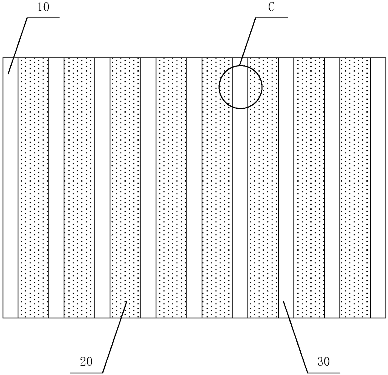
[0061] Figure 3-12 A schematic diagram of preparing a flexible array substrate for the first embodiment of the present invention, all of which are figure 2 Middle A-A sectional view. Among them, the "patterning process" mentioned in this embodiment includes deposition of film layer, coating of photoresist, mask exposure, development, etching, stripping of photoresist, etc., which is an existing mature preparation process. Deposition can use known processes such as sputtering, evaporation, and chemical vapor deposition, coating can use known coating processes, and etching can use known methods, which are not specifically limited here.

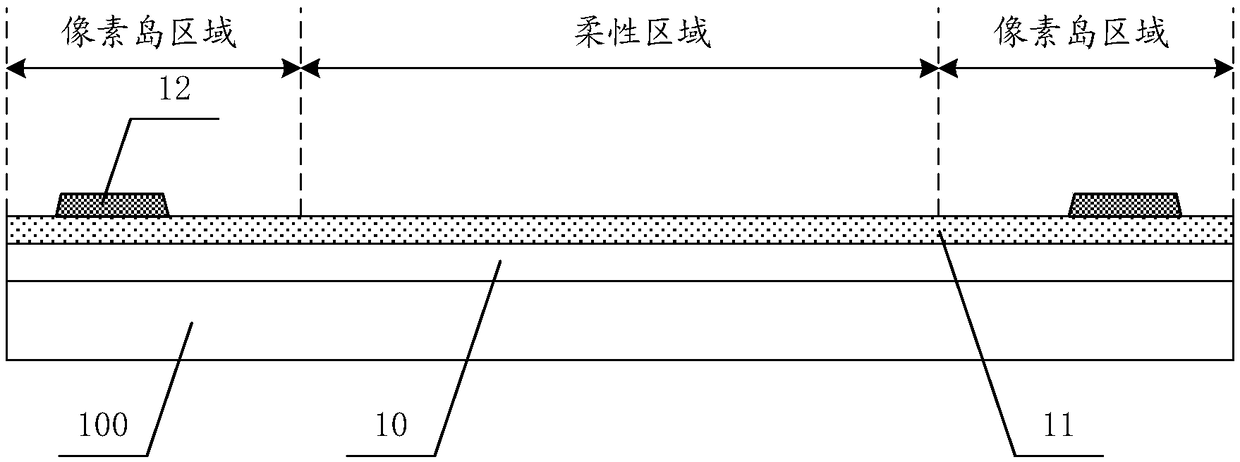
[0062] The technical solution of this embodiment will be described in detail below through the preparation process of the flexible array substrate. The overall process of preparing the flexible array substrate in this embodiment is as follows: first, the flexible substrate 10 is formed on the base substrate 100, and then structural layers su...

no. 2 example

[0091] Based on the technical concept of the present invention, an embodiment of the present invention also provides a method for preparing a flexible array substrate. Figure 13 It is a flow chart of the method for preparing the flexible array substrate in this embodiment. Such as Figure 13 Shown, the preparation method of flexible array substrate comprises:

[0092] S1. Forming an active layer, a gate insulating layer, a gate electrode and an interlayer insulating layer in several sequentially arranged pixel island regions;

[0093] S2. Form an elastic layer and connection lines in the flexible area between adjacent pixel island regions, and the connection lines are respectively connected to gate electrodes in adjacent pixel island regions.

[0094] Wherein, step S1 includes:

[0095] S11, sequentially forming an active layer, a gate insulating layer and a gate electrode on the flexible substrate;

[0096] S12. Form an interlayer insulating layer through a patterning pr...

no. 3 example

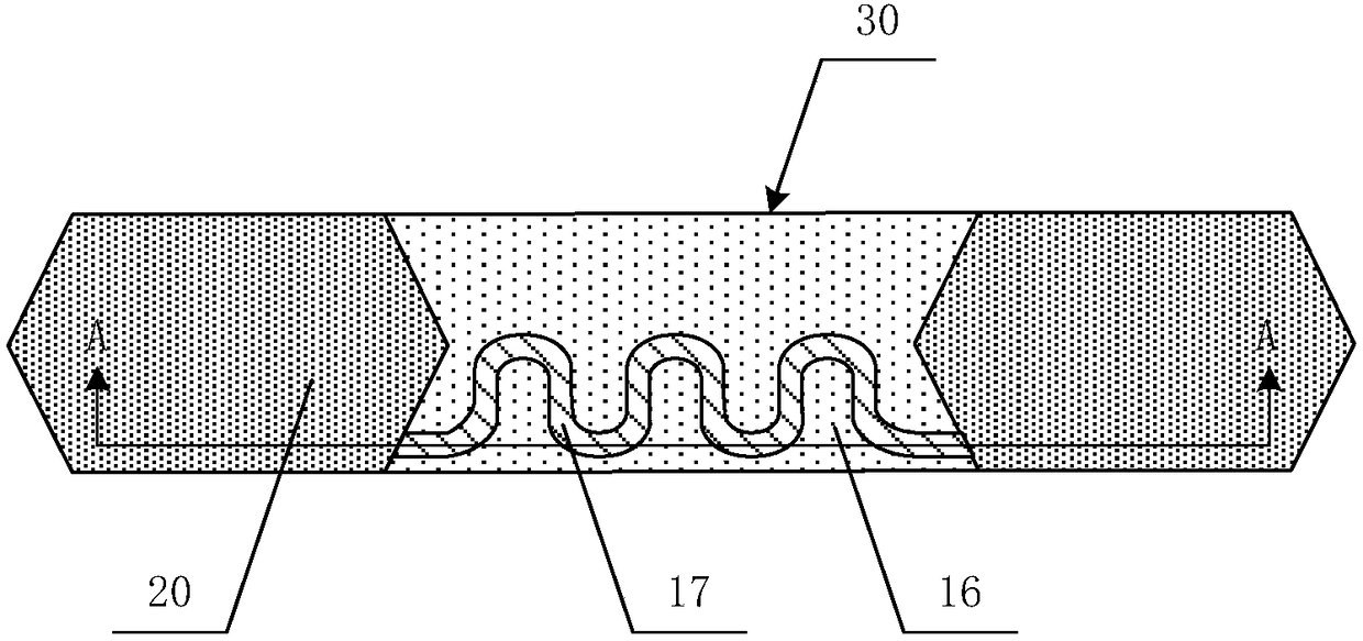
[0115] This embodiment is an extension based on the first embodiment. The difference from the first embodiment is that in this embodiment, the formation of the elastic layer and the data line pattern is realized by inkjet printing.

[0116] In this embodiment, the process from depositing the buffer layer to forming the pattern of the interlayer insulating layer is the same as that in the first embodiment. Forming the pattern of the elastic layer includes: forming the pattern of the elastic layer with connection grooves on the upper surface in the flexible channel 15b of the flexible area by inkjet printing. Since the inkjet printing method can pre-set the printing thickness of different areas, it is possible to reserve a rectangular or trapezoidal groove in the area where the connecting line pattern is located when printing the elastic layer. Subsequently, the conductive polymer is printed by inkjet printing to form a connection line pattern on the elastic layer, and the condu...


PUM

PropertyMeasurementUnit
Thicknessaaaaaaaaaa
Thicknessaaaaaaaaaa
Thicknessaaaaaaaaaa

Abstract

The invention provides a flexible array substrate, a preparation method thereof and a flexible display panel. The flexible array substrate comprises a plurality of pixel island regions which are sequentially arranged, and the adjacent pixel island regions are provided with a flexible region therebetween. Each pixel island region comprises an active layer, a gate insulating layer, a gate electrodeand an interlayer insulating layer which are arranged on a flexible substrate, each flexible region comprises an elastic layer and a connecting wire which are arranged on the flexible substrate, and the connecting wire is connected with the gate electrodes of the adjacent pixel island regions. According to the invention, the flexible array substrate is divided into a plurality of pixel island regions and a plurality of flexible regions, the pixel island regions are set to serve as pixel units of an effective display region, and the flexible regions serve as stretchable or bendable regions andare only provided with the elastic layer and the connecting wire, thereby effectively overcoming a problem that the insulating layer and grid lines of the existing structure are easy to break, being capable of ensuring the flexible regions to have sufficient stretching and bending performance, and realizing good stretching and bending performance of the flexible array substrate.

Description

technical field [0001] The invention relates to the field of display technology, in particular to a flexible array substrate, a preparation method thereof, and a flexible display panel. Background technique [0002] In the field of display technology, liquid crystal (Liquid Crystal Display, LCD) display devices and organic light emitting diode (Organic Light Emitting Diode, OLED) display devices have gradually replaced CRT displays. Because OLED display devices have the advantages of self-illumination, low driving voltage, high luminous efficiency, short response time, high definition and contrast, near 180° viewing angle, wide operating temperature range, etc., and can realize large-area full-color display, it is expected to become a successor The next-generation flat-panel display technology after the LCD display technology is one of the most concerned technologies in the flat-panel display technology. An active matrix organic light emitting diode (Active Matrix Organic L...

Claims


Application Information

Patent Timeline
IPC IPC(8): H01L27/32H01L27/10
CPCH01L27/10H10K59/00
Inventor 李小龙马伟欣李栋张帅
Owner BOE TECH GRP CO LTD
Why Eureka
Try Eureka