Deep ultraviolet LED packaging structure and manufacturing method thereof

An LED packaging and deep ultraviolet technology, applied in electrical components, circuits, semiconductor devices, etc., can solve the problems affecting the reliability and life of packaging devices, the decline in electrical conductivity, thermal conductivity and reflection performance, and the large difference in the refractive index of materials, and achieve a high level of improvement. Reliability and life indicators, avoiding total reflection, and improving the effect of device life

Active Publication Date: 2018-08-10
MAANSHAN JASON SEMICON CO LTD
View PDF5 Cites 14 Cited by
  • Summary
  • Abstract
  • Description
  • Claims
  • Application Information

AI Technical Summary

Problems solved by technology

[0006] The present invention provides a deep ultraviolet LED packaging structure and its manufacturing method, aiming to improve and solve the serious total reflection phenomenon caused by many material interfaces and large material refractive index differences under the existing packaging structure, and

Method used


Image

  • Deep ultraviolet LED packaging structure and manufacturing method thereof
  • Deep ultraviolet LED packaging structure and manufacturing method thereof
  • Deep ultraviolet LED packaging structure and manufacturing method thereof

Examples


Embodiment Construction

[0036] In order to make the purpose, technical solutions and advantages of the present invention clearer, the technical solutions in the present invention will be clearly and completely described below in conjunction with the embodiments of the present invention. Obviously, the described embodiments are part of the embodiments of the present invention. rather than all examples. Based on the embodiments of the present invention, all other embodiments obtained by persons of ordinary skill in the art without making creative efforts belong to the protection scope of the present invention.

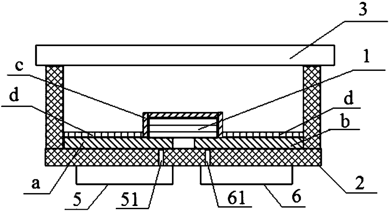
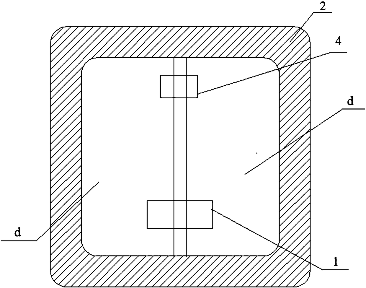
[0037] figure 1 It is a side cross-sectional view of an embodiment of the deep ultraviolet LED packaging structure of the present invention, figure 2 It is a top view of an embodiment of the deep ultraviolet LED packaging structure of the present invention, such as Figure 1-2 As shown, the present invention provides a deep ultraviolet LED packaging structure, including:

[0038] A deep ult...


PUM


Abstract

The invention provides a deep ultraviolet LED packaging structure and a manufacturing method thereof. The packaging structure comprises a deep ultraviolet LED chip and a bracket, an antireflection layer, a light-transmitting insulating layer and a light-transmitting cover plate, wherein the bracket has a downward concave hollow cavity with an upward opening; the inner bottom wall of the hollow cavity comprises a first coating region attached with a first metal layer and a second coating region attached with a second metal layer; the first coating region and the second coating region are arranged at intervals with different electrical properties; the deep ultraviolet LED chip stretches across between the first metal layer and the second metal layer; the antireflection layer is attached to the surface of the deep ultraviolet LED chip; the light-transmitting insulating layer is attached to regions, not in contact with the deep ultraviolet LED chip, on the outer surfaces of the first metallayer and the second metal layer; and the light-transmitting cover plate covers the opening of the bracket. By virtue of the deep ultraviolet LED packaging structure, occurrence of oxidization and corrosion phenomena of the metal material caused by exposure at a high temperature can be reduced; and in addition, a total reflection phenomenon of the LED chip light emitting surface caused by high material interface refractive index difference can be relieved.

Description

technical field [0001] The invention relates to LED packaging technology, in particular to a deep ultraviolet LED packaging structure and a manufacturing method thereof, belonging to the technical field of semiconductor device manufacturing. Background technique [0002] Ultraviolet light can usually be divided into: UVA (320-400nm), UVB (280-320nm), UVC (200-280nm) and vacuum ultraviolet VUV (10-200nm) according to the wavelength band. [0003] Ultraviolet light-emitting diodes (UV LEDs) based on III-nitride materials have broad application prospects in the fields of sterilization, polymer curing, biochemical detection, non-line-of-sight communication, and special lighting. Compared with the traditional ultraviolet light source mercury lamp, it has many advantages such as environmental protection, small and portable, low power consumption and low voltage. In recent years, it has received more and more attention and attention. [0004] As we all know, ultraviolet light has...

Claims


Application Information

Patent Timeline
IPC IPC(8): H01L33/48H01L33/62H01L33/44H01L33/00
CPCH01L33/0062H01L33/44H01L33/48H01L33/62H01L2933/0033H01L2933/0066
Inventor 姚禹郑远志陈向东梁旭东
Owner MAANSHAN JASON SEMICON CO LTD
Why Eureka
Try Eureka