A kind of dual function device based on gete and preparation method thereof

A dual-function, device technology, applied in the direction of electrical components, etc., can solve the problems of reducing the complexity of the storage density process, achieve good tolerance, low operating current, and increase the storage density.

Active Publication Date: 2020-04-03
HUBEI UNIV
View PDF3 Cites 0 Cited by
  • Summary
  • Abstract
  • Description
  • Claims
  • Application Information

AI Technical Summary

Problems solved by technology

However, this method of adding rectifier devices will undoubtedly reduce storage density and increase process complexity

Method used


Image

  • A kind of dual function device based on gete and preparation method thereof
  • A kind of dual function device based on gete and preparation method thereof
  • A kind of dual function device based on gete and preparation method thereof

Examples


Embodiment 1

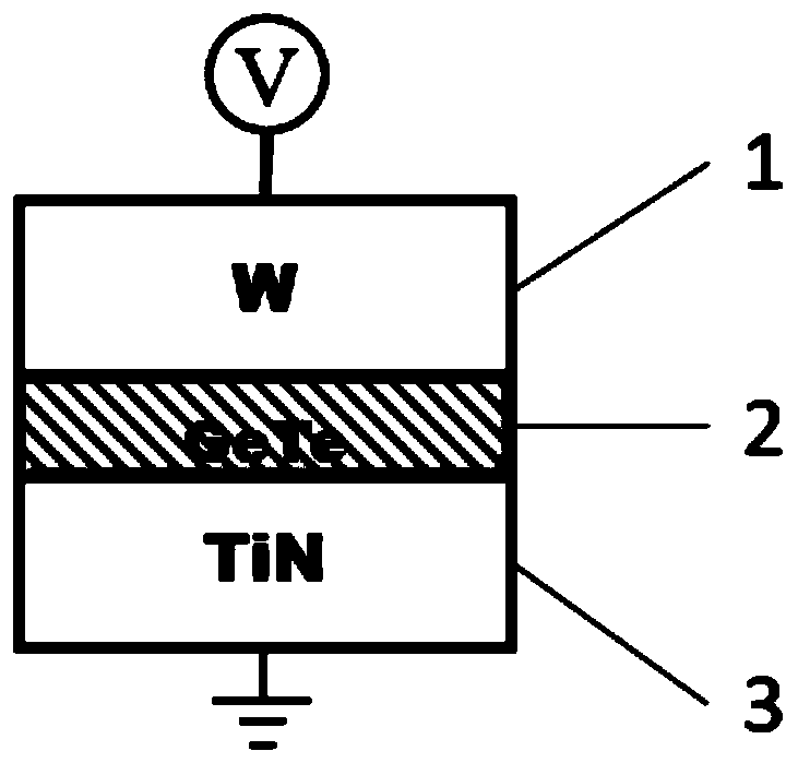
[0037] Such as figure 1 As shown, a GeTe-based bifunctional device in this embodiment includes a three-layer structure: a top electrode 1 , a thin film dielectric layer 2 and a bottom electrode 3 .

[0038] The bottom electrode 3 is made of TiN with a thickness of 200nm and a rectangular shape with a side length of 0.4 μm.

[0039] The GeTe thin film dielectric layer 2 has a thickness of 20 nm, a rectangular shape, and a side length of 0.4 μm.

[0040] The top electrode 1 is made of W with a thickness of 250 nm and a rectangular shape with a side length of 0.4 μm.

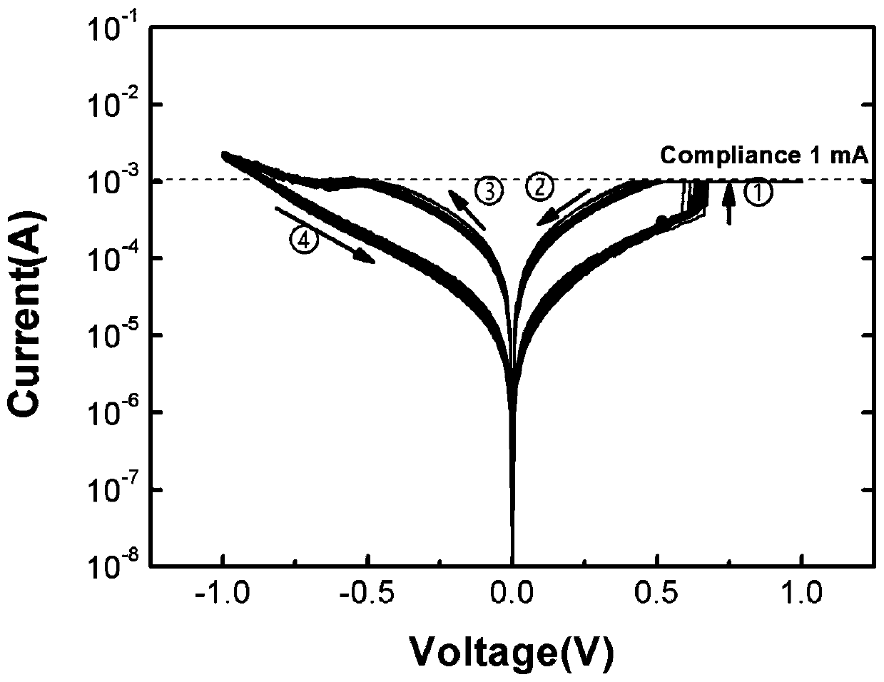
[0041] When realizing the conventional resistive switching function, the operating current limit range of the device is 1mA.

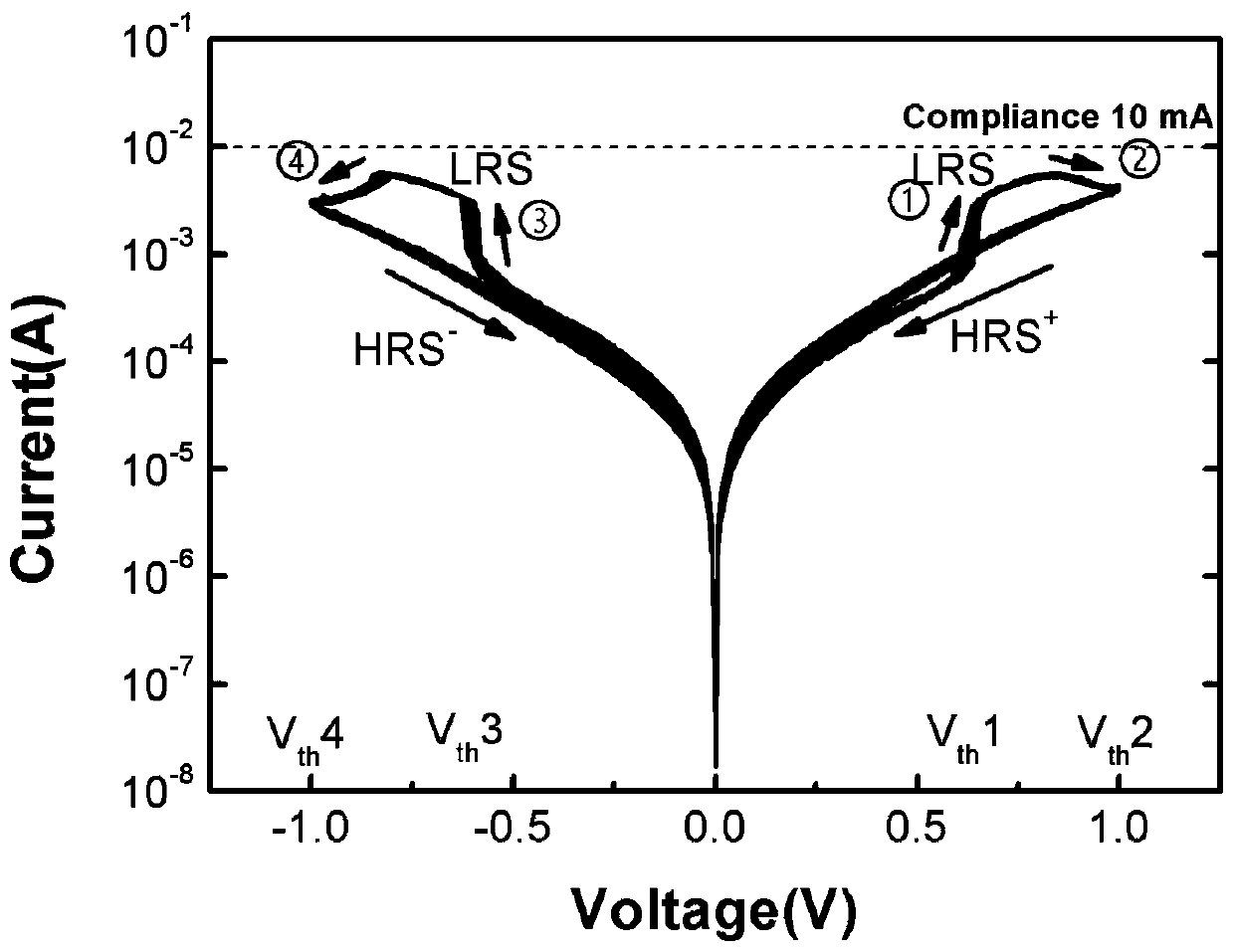
[0042] When realizing the complementary resistive switching function, the operating current limit range of the device is 10mA.

[0043] The preparation method of the GeTe-based dual-function device described above in this embodiment includes the following steps:

[0044] The bottom electr...

Embodiment 2

[0049] A GeTe-based dual-function device in this embodiment includes a three-layer structure: a top electrode, a thin-film dielectric layer, and a bottom electrode.

[0050] The bottom electrode is made of TiN with a thickness of 200 nm and a rectangular shape with a side length of 0.6 μm.

[0051] The dielectric layer of the GeTe thin film has a thickness of 20 nm and a rectangular shape with a side length of 0.6 μm.

[0052] The top electrode is made of W with a thickness of 250 nm and a rectangular shape with a side length of 0.6 μm.

[0053] When realizing the conventional resistive switching function, the operating current limit range of the device is 1mA.

[0054] When realizing the complementary resistive switching function, the operating current limit range of the device is 10mA.

[0055] The preparation method of the GeTe-based dual-function device described above in this embodiment includes the following steps:

[0056] The bottom electrode is prepared on the base...

Embodiment 3

[0061] A GeTe-based dual-function device in this embodiment includes a three-layer structure: a top electrode, a thin-film dielectric layer, and a bottom electrode.

[0062] The bottom electrode is made of TiN with a thickness of 200 nm and a rectangular shape with a side length of 0.8 μm.

[0063] The dielectric layer of the GeTe thin film has a thickness of 20 nm and a rectangular shape with a side length of 0.8 μm.

[0064] The top electrode is made of W with a thickness of 250 nm and a rectangular shape with a side length of 0.8 μm.

[0065] When realizing the conventional resistive switching function, the operating current limit range of the device is 1mA.

[0066] When realizing the complementary resistive switching function, the operating current limit range of the device is 10mA.

[0067] The preparation method of the above-mentioned GeTe-based dual-function device comprises the following steps:

[0068] The bottom electrode is prepared on the base; a GeTe thin film...


PUM

PropertyMeasurementUnit
thicknessaaaaaaaaaa
thicknessaaaaaaaaaa
lengthaaaaaaaaaa

Abstract

The invention discloses a GeTe-based dual-function device and a preparation method thereof. The device includes a three-layer structure: a top electrode, a thin-film dielectric layer and a bottom electrode. The top electrode is W; the thin film dielectric layer is GeTe thin film; the material of the bottom electrode is any one selected from ITO, FTO, ZTO, TaN or TiN. The top electrode, the thin film dielectric layer and the bottom electrode are all prepared by magnetron sputtering. By controlling the size of the operating current, the GeTe thin film dielectric layer can be switched in different resistance states, so as to realize the conventional resistance switching function or the complementary resistance switching function. The conventional resistive switching function of the dual-function device proposed by the present invention can be used as a conventional memory storage element, and the complementary resistive switching function can effectively solve the current crosstalk problem in the cross array of resistive variable memory. By reasonably controlling the size of the operating current, the The mutual conversion of the two functions greatly improves the application range of the device.

Description

technical field [0001] The invention relates to the field of novel micro-nano electronic materials and functional devices, in particular to a GeTe-based dual-functional device and a preparation method thereof. Background technique [0002] Resistive random access memory (RRAM) is considered as one of the candidates for the next generation of nonvolatile memory (NVM) because of its simple device structure, excellent scalability, high switching speed and excellent data retention. RRAM has good compatibility with complementary metal-oxide-semiconductor (CMOS) technology, so it is easy to construct a 3D crossbar array (CrossbarArray) structure to achieve high-density storage. However, one of the main disadvantages of this structure is that adjacent memory cells are prone to crosstalk, especially when reading in a low-resistance state. This problem has the potential to cause memory addressing and reading errors, increases power consumption, and limits the integration of the cros...

Claims


Application Information

Patent Timeline
Patent Type & Authority Patents(China)
IPC IPC(8): H01L45/00
CPCH10N70/24H10N70/8416H10N70/026H10N70/8828
Inventor 王浩何玉立马国坤刘春雷陈傲陈钦
Owner HUBEI UNIV
Why Eureka
Try Eureka