

A method for establishing multiphysics coupled large-signal model of gan HEMT device
A model-building, large-signal technology, applied in instrumentation, electrical digital data processing, special data processing applications, etc., can solve the problems of low model accuracy and incomplete description of multi-physics coupling effects, and achieve the effect of improving accuracy
- Summary
- Abstract
- Description
- Claims
- Application Information
AI Technical Summary
Problems solved by technology
Method used
Image

Examples
Embodiment Construction
[0050] Further describe the technical scheme of the present invention in detail below in conjunction with accompanying drawing:
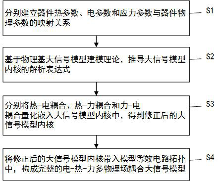
[0051] Such as figure 1 As shown, a GaN HEMT device multi-physics coupling large-signal model establishment method includes the following steps:
[0052] S1: Establish the mapping relationship between the thermal parameters, electrical parameters and stress parameters of the device and the physical parameters of the device respectively.
[0053] This example adopts the research methods of theoretical and method research combined with experimental verification, and proposes a research method starting from the theory of quantum mechanics, cross-fusion thermodynamics, classical mechanics, semiconductor physics and other multidisciplinary theories, and establishes the thermal parameters and electrical parameters of GaNHEMT devices respectively. And the mapping relationship between stress parameters and device physical parameters. Among them, preferabl...
PUM
 Abstract
Description
Claims
Application Information