Quantum chip port impedance test device and test method

A technology of impedance testing and chips, which is applied in the direction of measuring devices, measuring resistance/reactance/impedance, measuring electrical variables, etc., can solve the problems of low test accuracy, quantum chips are easy to be broken down, and manual test efficiency, so as to improve test efficiency, The effect of convenient and quick measurement and reducing the chip damage rate

Pending Publication Date: 2018-08-24
ORIGIN QUANTUM COMPUTING TECH (HEFEI) CO LTD
View PDF7 Cites 9 Cited by
  • Summary
  • Abstract
  • Description
  • Claims
  • Application Information

AI Technical Summary

Problems solved by technology

[0006] The present invention provides a convenient quantum chip port impedance testing device and measurement method for the problems of low test accuracy, easy breakdown of the quantum chip and low manual test efficiency of the device and method for measuring the impedance of the quantum chip in the prior art.

Method used


Image

  • Quantum chip port impedance test device and test method
  • Quantum chip port impedance test device and test method
  • Quantum chip port impedance test device and test method

Examples


Embodiment 1

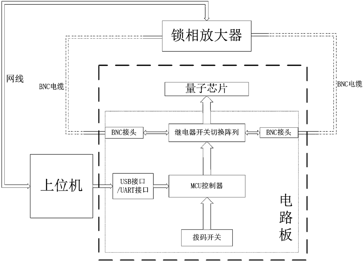
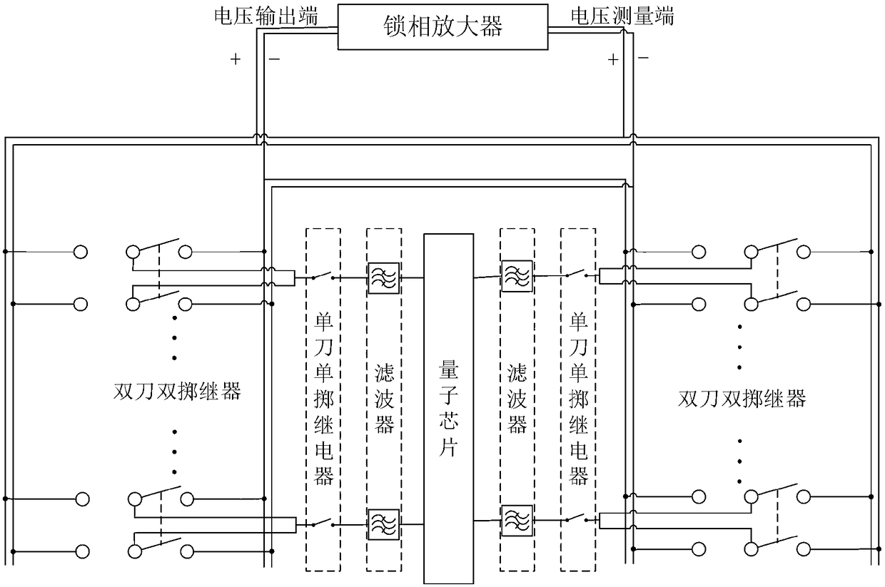
[0043] refer to figure 1 and figure 2 , A quantum chip port impedance test device, including a lock-in amplifier, a relay array switching circuit, a quantum chip, an MCU controller, and a host computer, the output end of the lock-in amplifier is connected to the input end of the relay array switching circuit, and the relay array switching circuit. The output end is connected to the input end of the lock-in amplifier, and the lock-in amplifier is used to provide small voltage output and small voltage measurement, which is used to meet the requirement of extremely low test voltage between the ports of the quantum chip and to improve the test accuracy. Each channel of the relay array switching circuit is connected to each port of the quantum chip, and the switching circuit of the relay array switching circuit is used to realize the switching of the voltage output terminal and the voltage detection terminal of the lock-in amplifier to the port channel of each quantum chip, instea...

Embodiment 2

[0049] refer to figure 2 The difference from Embodiment 1 is that each double-pole double-throw relay of the relay array switching circuit is connected to a single-channel filter, and the single-channel filter is connected to a single port of the quantum chip.

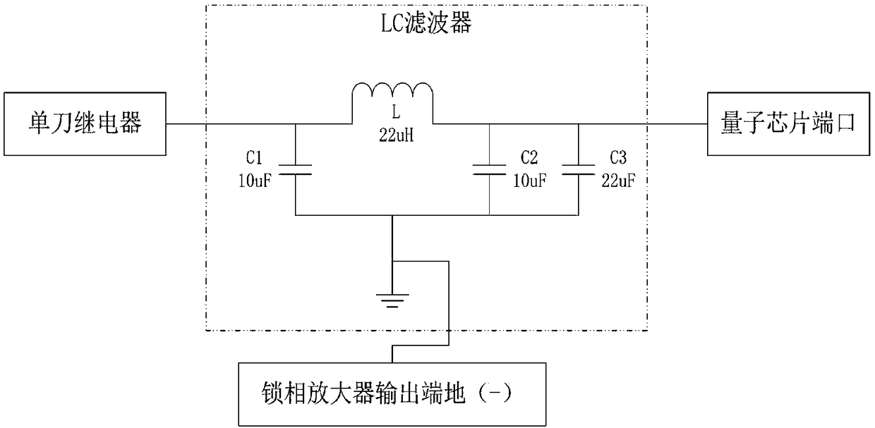
[0050] refer to image 3 , the filter structure and connection mode are shown in the figure, each channel of the relay array switching circuit is connected to a single channel filter, and the single channel filter is connected to a single port of the quantum chip. The form of the filter between the SPST relay and the quantum chip port is a 3-stage Butterworth low-pass LC filter, which is composed of a 10uF capacitor C1, a 22uH inductor L, a 10uF capacitor C2 and a 22uF capacitor C3. The ground terminal of the filter should be connected to the low potential (-) of the output terminal of the lock-in amplifier. The connection of the filter has a good effect on suppressing the electromagnetic interference of the relay an...

Embodiment 3

[0053] In this embodiment, the circuit structure is basically the same as the above-mentioned embodiment, the difference is that the relay array switching circuit also includes a single-pole relay, and the relay array is composed of a plurality of double-pole double-throw relays and single-pole single-throw relays. The ports correspond to a double-pole double-throw relay and a single-pole single-throw relay respectively, and the double-pole double-throw relay is connected to the quantum chip port through the single-pole relay. In this way, high-level, low-level and floating high-impedance states can be provided for each quantum chip port, and the impedance between several ports can be tested more conveniently and flexibly.

[0054] figure 2 The connection method between the lock-in amplifier and the relay array, the connection method between the relay array and the filter, the connection method between the filter and the quantum chip, and the composition method of the entire ...


PUM


Abstract

The invention discloses a quantum chip port impedance test device and a test method, and belongs to the field of quantum. The accurate and convenient quantum chip port impedance test device comprisesa lock-in amplifier, a relay array switching circuit, a quantum chip, an MCU controller and an upper computer. Each path of the relay array switching circuit is connected with each port of the quantumchip. The relay array switching circuit comprises a double-pole double-throw relay. The double-pole double-throw relay is connected with the MCU controller. The MCU controller is connected with the upper computer. The test method comprises the following steps: outputting and adjusting a signal of the lock-in amplifier to the minimum voltage, outputting and adjusting the signal of the lock-in amplifier to a test voltage value, opening a communication program of the upper computer, connecting ports, needing to be tested, of the quantum chip in sequence, and collecting the voltage data and the current data by using a lock-in amplifier program of the upper computer. The test device and the test method have the advantages of being high in testing efficiency and convenient to operate, and avoiding breakdown of the quantum chip.

Description

technical field [0001] The invention relates to the field of quantum chips, in particular to a quantum chip port impedance testing device and a measurement method. Background technique [0002] In the field of quantum chips, quantum chip port impedance is an important external characterization of quantum chip device parameter performance. Current methods of measuring resistance are not fully applicable to measuring quantum chips, because quantum chip measurements require extremely small voltages. Generally, the voltmeter cannot be tested directly, and the noise is also greatly affected by the measurement after amplification. If a traditional universal multimeter is used to directly measure the quantum chip, some ports of the quantum chip will be directly broken down. If a general bridge instrument is used, there will also be an uncertain voltage relative to the withstand voltage of the quantum chip. Using general voltammetry to measure the resistance will bring about the r...

Claims


Application Information

Patent Timeline
Patent Type & Authority Applications(China)
IPC IPC(8): G01R27/08
CPCG01R27/08
Inventor 贾志龙陈华鹏
Owner ORIGIN QUANTUM COMPUTING TECH (HEFEI) CO LTD
Why Eureka
Try Eureka