A plastic packaging method to solve the mold flow problem of plastic packaging and widen the width of wafers

A wafer and problem-solving technology, applied in the field of plastic packaging to solve the problem of plastic packaging mold flow and widen the width of wafers

Active Publication Date: 2019-08-06
上海飞骧电子科技有限公司
View PDF3 Cites 0 Cited by
  • Summary
  • Abstract
  • Description
  • Claims
  • Application Information

AI Technical Summary

Problems solved by technology

The traditional plastic encapsulation process is only suitable for side-mounted wafers with long sides attached to the carrier board design, and the wafer width perpendicular to the carrier board is best within 500 microns

Method used


Image

  • A plastic packaging method to solve the mold flow problem of plastic packaging and widen the width of wafers
  • A plastic packaging method to solve the mold flow problem of plastic packaging and widen the width of wafers
  • A plastic packaging method to solve the mold flow problem of plastic packaging and widen the width of wafers

Examples


Embodiment Construction

[0038] The specific embodiments of the present invention will be described in more detail below with reference to the drawings and examples, so as to better understand the solution of the present invention and its advantages in various aspects. However, the specific embodiments and examples described below are for the purpose of illustration only, rather than limiting the present invention.

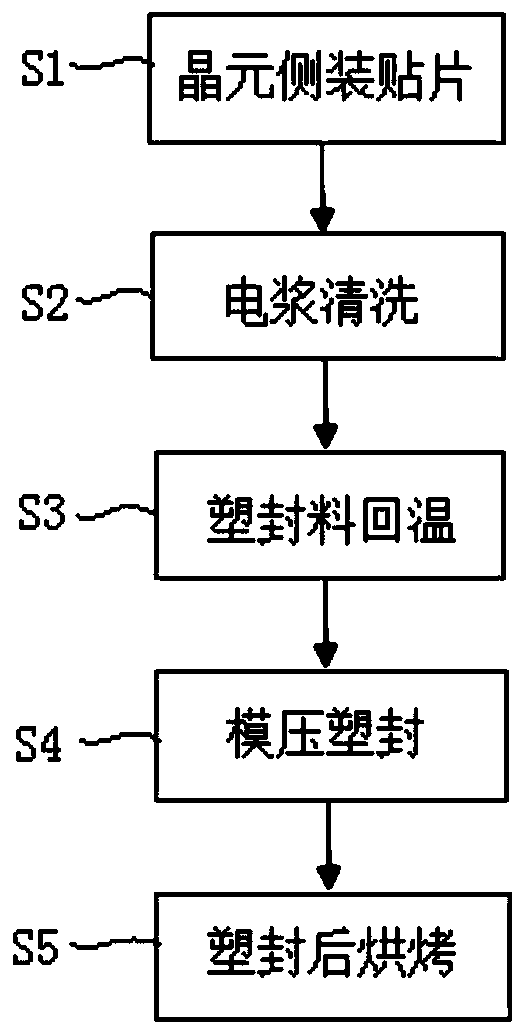
[0039] A plastic packaging method to solve the mold flow problem of plastic packaging and widen the width of wafers, such as figure 1 as shown, figure 1 It is a schematic flow chart of the method of the present invention. The method includes the following steps.

[0040] Step S1, designing the wafer circuit, and side-mounting the wafer and the carrier board.

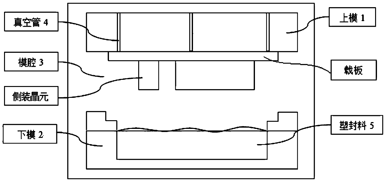
[0041] image 3 It is a schematic diagram of floor mount plastic package of the present invention. Such as image 3 As shown, the wafer circuit design adopts one of single-sided circuit design or double-sided circuit design. ...


PUM

PropertyMeasurementUnit
heightaaaaaaaaaa
sizeaaaaaaaaaa

Abstract

A plastic packaging method comprises the following steps: designing a die circuit, and side mounting a die to a carrier using a plasma to clean the carrier and a surface of the die; increasing the temperature of a powdery plastic packaging material; performing press molding to plastic-package the carrier mounted with the die; and heating the plastic-packaged carrier.

Description

technical field [0001] The invention relates to the field of semiconductor manufacturing, in particular to a plastic packaging method for solving the mold flow problem of plastic packaging and widening the width of wafers. Background technique [0002] Wafer is the carrier used in the production of integrated circuits. It mostly refers to single crystal silicon wafers, as well as compound wafers such as gallium arsenide, silicon carbide, gallium nitride, and indium phosphide. In the semiconductor manufacturing process, wafers are usually designed and manufactured on a single side. However, as the demand for various functional integrations increases and becomes higher and higher, the requirements for transistor integration density become higher and higher, which becomes more and more challenging. [0003] Chip packaging, the current industry often adopts front-mount or flip-chip. Compared with the traditional method of front-mount or flip-chip, the main difference is that th...

Claims


Application Information

Patent Timeline
Patent Type & Authority Patents(China)
IPC IPC(8): B29C43/18B29C43/56B29C43/52H01L21/56
CPCB29C43/18B29C43/52B29C43/56B29C2043/181B29C2043/563H01L21/561B29C43/006B29L2031/3481H01L21/56H01L21/565
Inventor 吴现伟龙华郭嘉帅郑瑞
Owner 上海飞骧电子科技有限公司
Why Eureka
Try Eureka