Image sensor and forming method thereof

An image sensor and patterning technology, applied in the direction of electric solid-state devices, semiconductor devices, electrical components, etc., can solve problems such as hard mask layer cracking, impact on the quality of subsequent process products, and affect the quality of subsequent process products, etc., to achieve smooth appearance Effect

Inactive Publication Date: 2018-08-31
HUAIAN IMAGING DEVICE MFGR CORP
View PDF4 Cites 1 Cited by
  • Summary
  • Abstract
  • Description
  • Claims
  • Application Information

AI Technical Summary

Problems solved by technology

[0004] However, in the prior art, the hard mask layer is prone to cracking at the top opening of the etched trench, which affects subsequent processes and product quality, and the dielectric layer is prone to cracking at the top of the etched trench. Closure phenomenon, the formation of dielectric holes in the etching trench, will further affect the subsequent process and product quality

Method used


Image

  • Image sensor and forming method thereof
  • Image sensor and forming method thereof
  • Image sensor and forming method thereof

Examples


Embodiment Construction

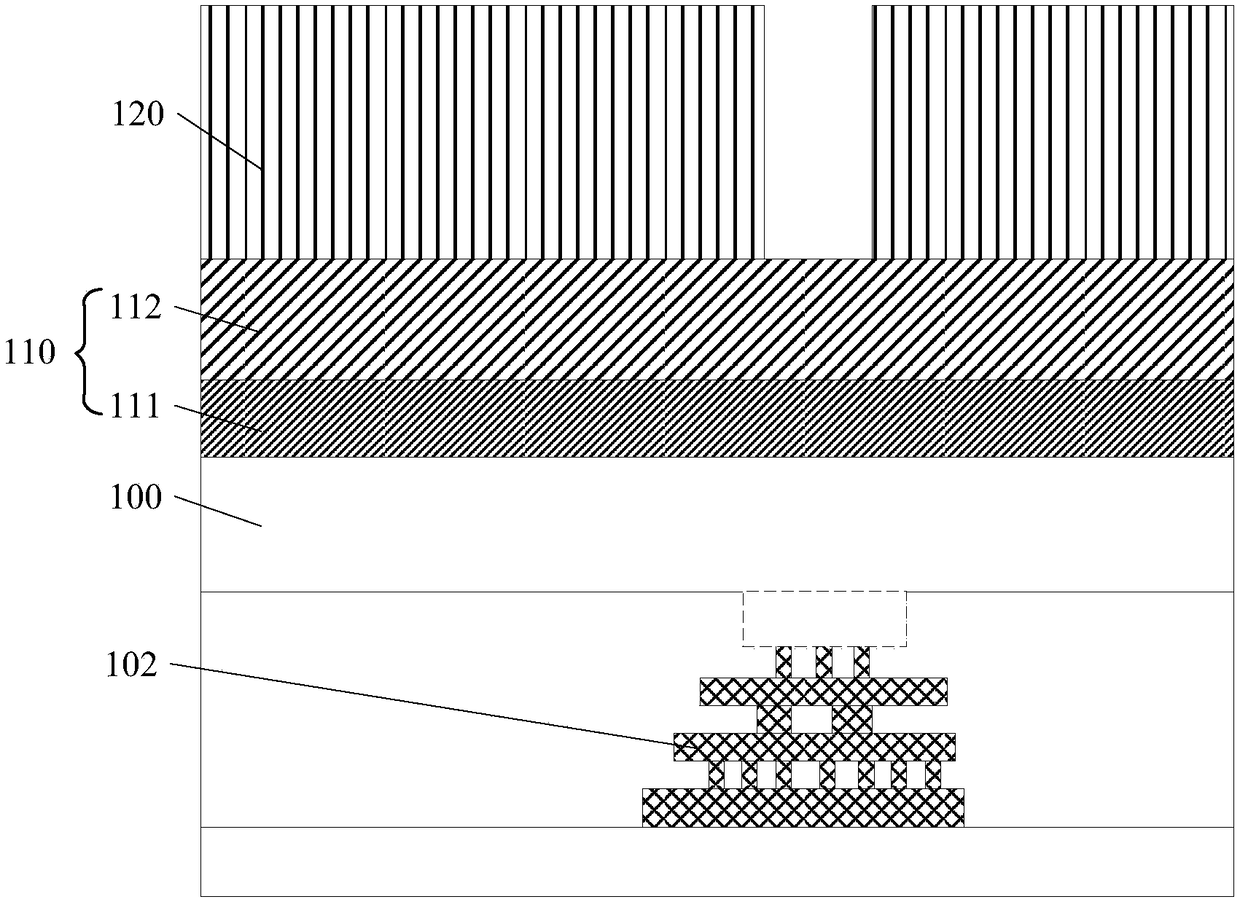
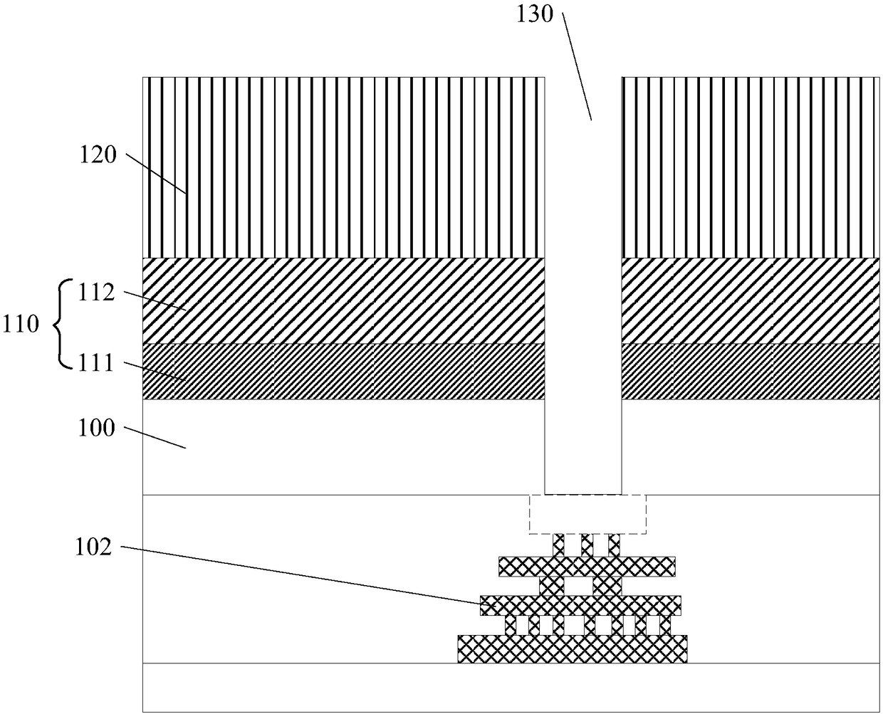
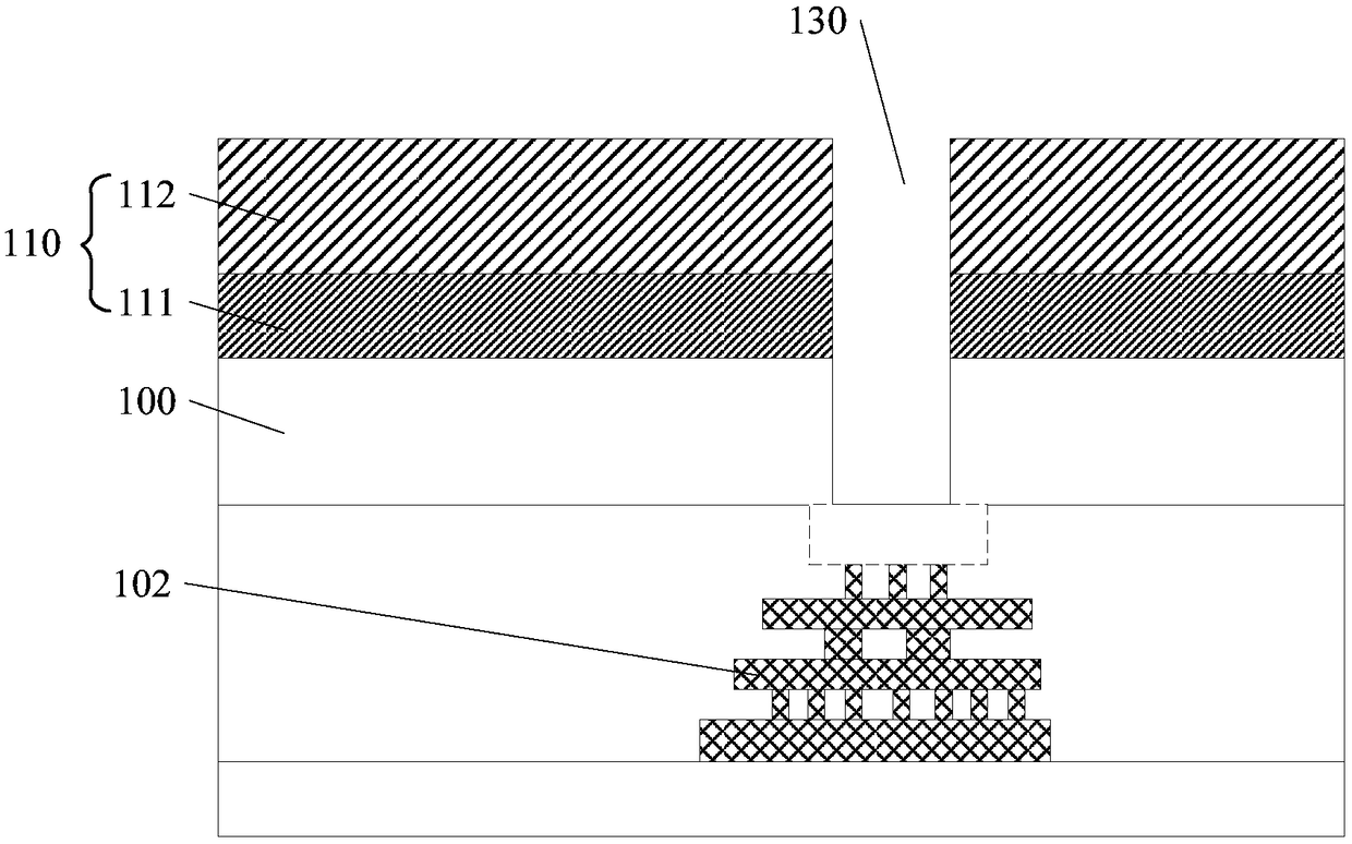
[0024] In the prior art, a process of filling a dielectric layer in a trench generally includes the following steps: forming a hard mask layer on the surface of a semiconductor substrate, and then etching the hard mask layer to form a etching grooves extending in the direction of the semiconductor substrate, and then forming a dielectric layer covering the etching grooves.

[0025] refer to Figure 1 to Figure 4 , Figure 1 to Figure 4 It is a schematic diagram of a cross-sectional structure of a device corresponding to each step in a method for forming an image sensor in the prior art.

[0026] refer to figure 1 , providing a semiconductor substrate 100, a hard mask layer 110 is formed on the back of the semiconductor substrate 100, a front structure 102 is formed on the front of the semiconductor substrate 100, and a patterned pattern is formed on the surface of the semiconductor substrate 100. The mask layer 120.

[0027] In a specific implementation, the front structure...


PUM


Abstract

The invention discloses an image sensor and a forming method thereof. The method comprises the following steps: providing a semiconductor substrate, wherein a hard mask layer is formed on the back ofthe semiconductor substrate, and a front structure is formed on the front of the semiconductor substrate; forming a graphical mask layer, and etching the hard mask layer according to the mask layer soas to form an etching groove, wherein the etching groove runs through the hard mask layer, the side wall of the etching groove comprises an upper side wall and a lower side wall which are connected vertically, and the included angle between the upper side wall and the surface of the hard mask layer is an obtuse angle; taking the mask layer as a mask, and etching the semiconductor substrate so that the etching groove runs through the semiconductor substrate; forming a dielectric layer, wherein the bottom and the side wall of the etching groove are covered with the dielectric layer, and the hard mask layer is covered with the dielectric layer. Through the scheme, the possibility of the cracking problem for the hard mask layer can be reduced.

Description

technical field [0001] The invention relates to the technical field of semiconductor manufacturing, in particular to an image sensor and a forming method thereof. Background technique [0002] In the existing semiconductor manufacturing process, there is a process of filling the dielectric layer in the trench. For example, in the manufacturing process of a CMOS image sensor (CMOS Image Sensors, CIS) device, it can be formed on the front side of the semiconductor substrate first. Logic devices, pixel devices, and metal interconnection structures, etc., are then bonded to the front side of the semiconductor substrate using a carrier wafer, and then on the back side of the semiconductor substrate to form through holes (Through Silicon Via, TSV), filter (Filter ) and other structures. [0003] Specifically, in the existing process of forming TSVs, a hard mask layer is usually formed on the surface of the semiconductor substrate, and then the hard mask layer is etched to form TS...

Claims


Application Information

Patent Timeline
Patent Type & Authority Applications(China)
IPC IPC(8): H01L27/146
CPCH01L27/1462H01L27/14683H01L27/14685
Inventor 李晓明林宗德何延强
Owner HUAIAN IMAGING DEVICE MFGR CORP
Why Eureka
Try Eureka