Periodic cross waveguide structure, electro-optical modulation structure and MZI (Mach-Zehnder Interference) structure

A technology of waveguide structure and electro-optical modulation, which is applied in the fields of nonlinear optics, optics, instruments, etc., can solve the problems that it is difficult to further improve the performance of modulation devices and the weak plasma dispersion effect, so as to improve the working speed of devices, excellent modulation function, and low refractive index. The effect of increasing the change

Active Publication Date: 2018-09-04
INST OF SEMICONDUCTORS - CHINESE ACAD OF SCI
View PDF5 Cites 1 Cited by
  • Summary
  • Abstract
  • Description
  • Claims
  • Application Information

AI Technical Summary

Problems solved by technology

[0004] At present, in the traditional silicon-based electro-optic modulators, there are electro-optic modulators with two-finger equal-height insertion type reverse-biased pn junction waveguides with high working speed and high efficiency, but due to the silicon material due to its plasmonic dispersion The effect is weak (at a carrier concentration change of 1×10 17 ~1×10 18 cm -3 In the case of a change in refractive index of 1×10 -4 ~3×10 -3 )’s own disadvantages, for example, to achieve π-phase modulation in traditional silicon-based MZI electro-optic modulators, a higher modulation voltage is required for the phase-shifting arm (also known as the modulation arm), which makes it difficult to further improve the performance of the modulation device

Method used


Image

  • Periodic cross waveguide structure, electro-optical modulation structure and MZI (Mach-Zehnder Interference) structure
  • Periodic cross waveguide structure, electro-optical modulation structure and MZI (Mach-Zehnder Interference) structure
  • Periodic cross waveguide structure, electro-optical modulation structure and MZI (Mach-Zehnder Interference) structure

Examples


Embodiment Construction

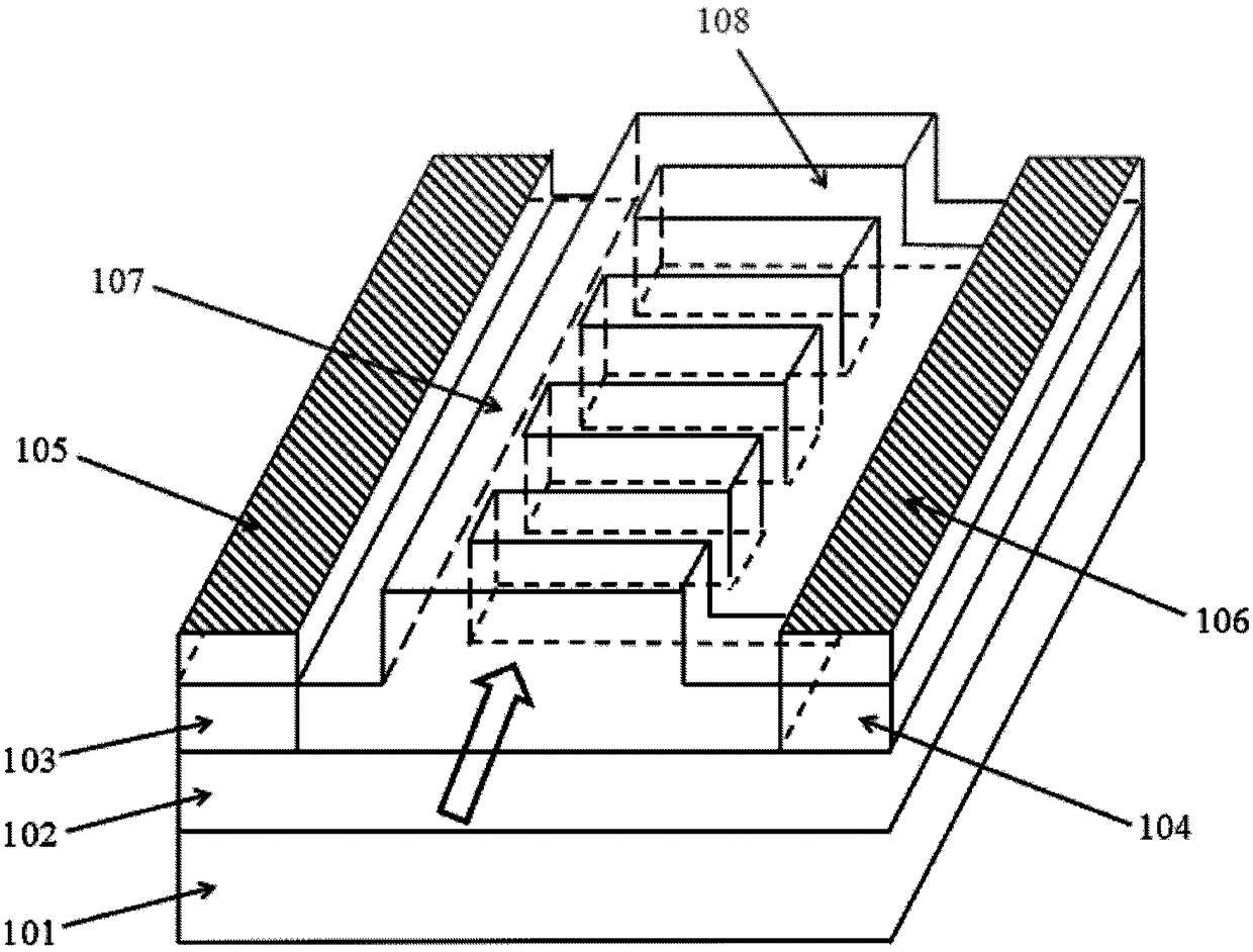
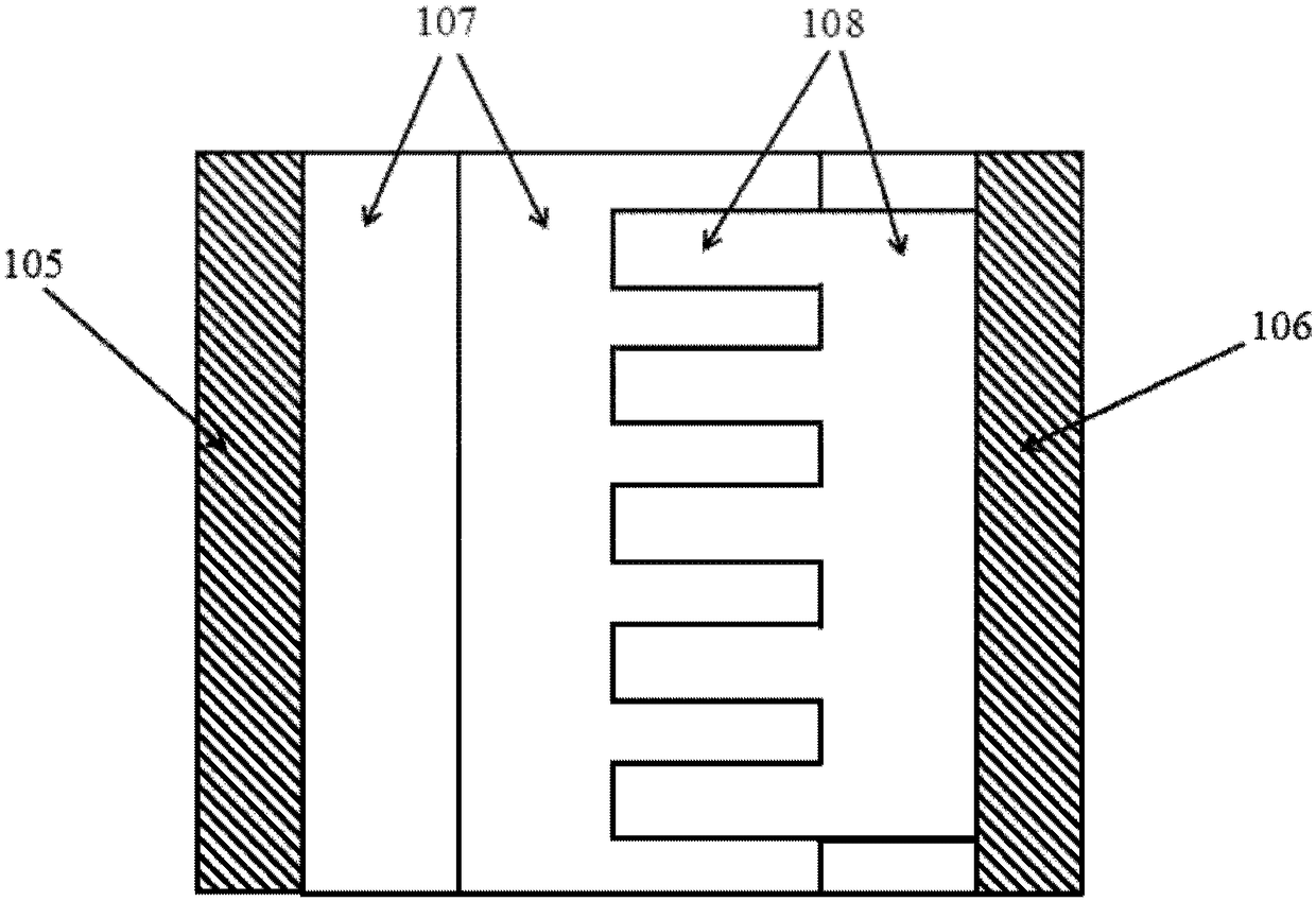
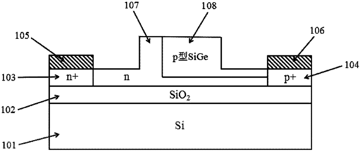
[0029]The applicant of the present invention has found through determined research that the carrier effective mass of SiGe material is smaller than that of Si material, and the adjustment of its material bandgap and the change of other parameters can be realized by technologies such as strain engineering, so that SiGe or Ge / The plasma dispersion effect in the SiGe quantum well will be effectively enhanced, and the manufacturing process is compatible with the traditional CMOS process. On this basis, a new reasonable waveguide structure is designed by introducing SiGe material into silicon-based SOI material.

[0030] To this end, the present invention provides a novel periodic interleaved waveguide structure as a rational waveguide structure based on Si / SiGe materials, and an electro-optical modulation structure and an MZI structure using it, wherein, in the periodically interleaved waveguide structure, periodic Si-doped regions and SiGe-doped regions are arranged alternately,...


PUM

PropertyMeasurementUnit
thicknessaaaaaaaaaa
refractive indexaaaaaaaaaa

Abstract

The invention provides a periodic cross waveguide structure, and an electro-optical modulation structure and an MZI (Mach-Zehnder Interference) structure both utilizing the same. The periodic cross waveguide structure is in the shape of ridge; strip-like interdigital n-type Si doped zones are formed at position, along a waveguide extension direction, at the ridge-shaped waveguide center; p-type SiGe doped zones are formed among the interdigital spaces; the n-type Si doped zones and the p-type SiGe doped zones are arranged in a periodic cross manner; the n-type Si doped zones are connected at one side of the interdigital spaces thereof and are connected with the bottom of the ridge-shaped waveguide center; gaps are formed between the interdigital bottoms of the n-type Si doped zones and theupper surface of the n-type Si doped zones connected at the bottom of ridge-shaped waveguide center, the p-type SiGe doped zones are arranged in the gaps, and thus, the p-type SiGe zones formed amongthe interdigital spaces are connected mutually. SiGe material carrier effective mass is reduced, free carrier plasma dispersion effect is improved, change of reflective index of the SiGe material isincreased, and accordingly, modulation efficiency, modulation speed, and modulation power consumption are optimized, and the effect of reducing size while improving modulation performance is achieved.

Description

technical field [0001] The invention belongs to the field of silicon-based optoelectronic devices, in particular to a periodically interleaved waveguide structure, an electro-optic modulation structure using it and a Mach-Zehnder interference (MZI) structure, in particular to a material capable of enhancing The refractive index change of the dispersion effect increases the modulation efficiency, improves the working speed of the device, reduces the power consumption of the device, and periodically interleaves the waveguide structure, as well as the electro-optic modulation structure and the MZI structure using it. Background technique [0002] With the rapid development of the information age, the optical modulator is an important component of the transmitting end of the communication system in the optical communication technology. Generally, photonic components used to realize the functions of transmission, generation, processing and detection of optical signals mainly incl...

Claims


Application Information

Patent Timeline
Patent Type & Authority Applications(China)
IPC IPC(8): G02F1/035G02F1/21
CPCG02F1/035G02F1/21G02F1/212
Inventor 匡迎新李智勇刘阳刘磊李泽正
Owner INST OF SEMICONDUCTORS - CHINESE ACAD OF SCI
Why Eureka
Try Eureka