Method and device for checking repeated resistance in printed circuit board
A technology of printed circuit boards and circuit boards, which is applied to the layout inspection of printed circuit boards and the field of repetitive resistance inspection in printed circuit boards. It can solve problems such as low efficiency and easy missed inspections, so as to improve work efficiency and reduce processing cost, and the effect of reducing design difficulty
- Summary
- Abstract
- Description
- Claims
- Application Information
AI Technical Summary
Problems solved by technology
Method used
Image

Examples
Embodiment Construction
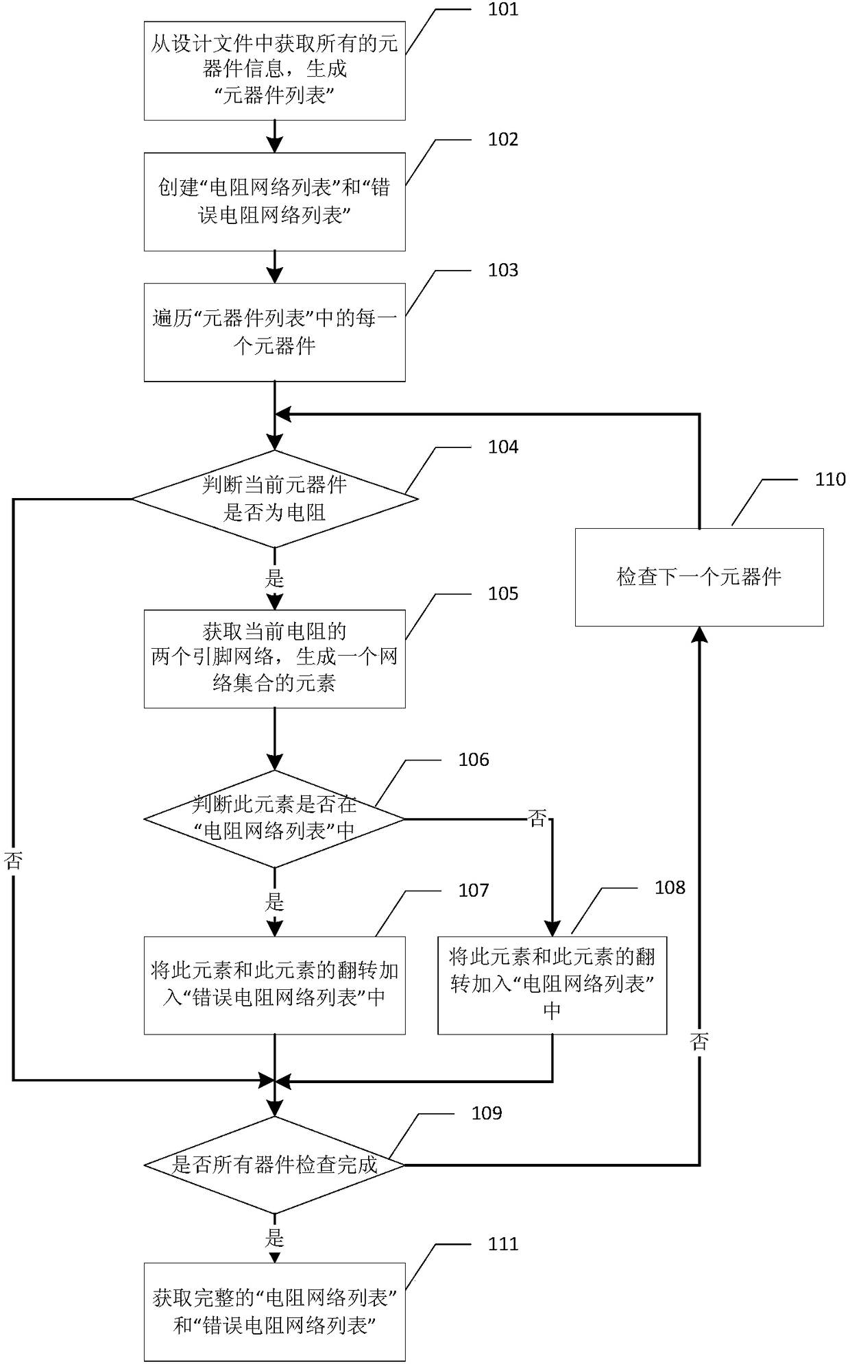
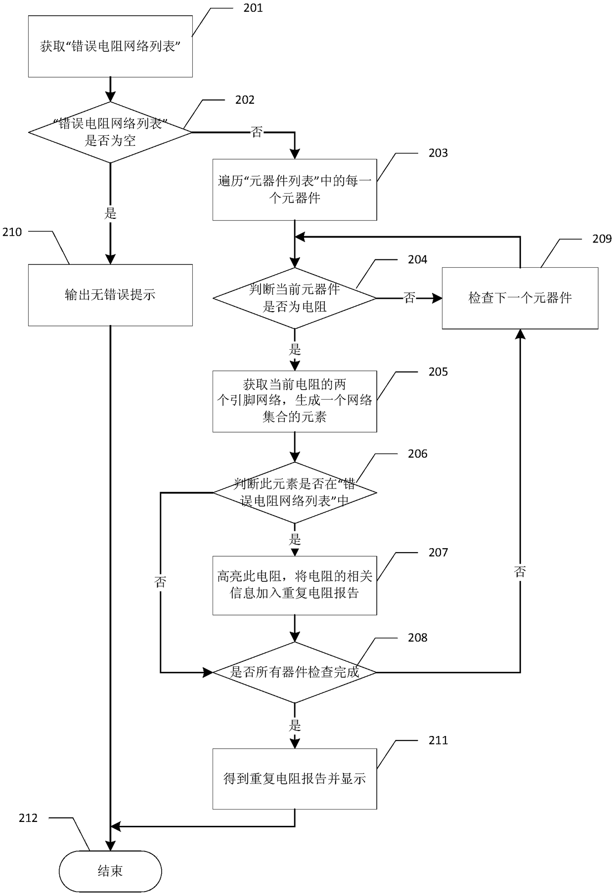
[0054] In view of the deficiencies in the prior art, the inventor of this case was able to propose the technical solution of the present invention after long-term research and extensive practice. The technical solution, its implementation process and principle will be further explained as follows.
[0055] The invention writes a program file for checking the repeated resistance in the printed circuit board and saves it as a callable file format of the circuit board design software, and the circuit board design software calls the program file to perform the repeated resistance check.
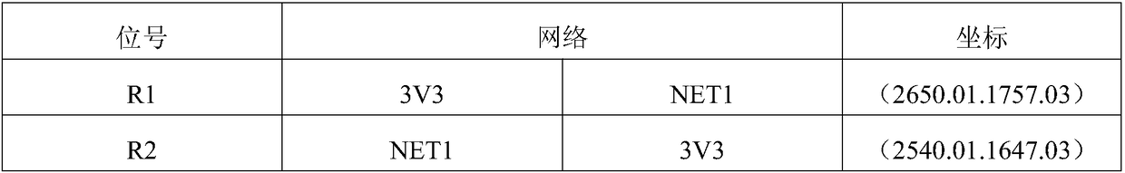
[0056] Common printed circuit board (Printed Circuit Board, PCB) design software includes Protel, Mentorpads, Cadence Allegro, etc. Taking Cadence Allegro software as an example, the inspection of PCB design can be realized through the secondary development of its SKILL platform. For example, in the embodiment of the present invention, the SKILL program for checking the repeated resistance in the...
PUM
 Abstract
Description
Claims
Application Information