Manufacturing methods of electrolytic copper foil having needle-shaped copper particles and circuit board assembly

A technology of electrolytic copper foil and manufacturing method, which is applied in the field of manufacturing electrolytic copper foil and circuit board components, can solve the problems of reducing the peel strength of copper foil and circuit substrate, insufficient peel strength of copper foil, etc., and achieve high peel strength and large contact area effect

Pending Publication Date: 2018-09-07
NANYA PLASTICS CORP
View PDF7 Cites 2 Cited by
  • Summary
  • Abstract
  • Description
  • Claims
  • Application Information

AI Technical Summary

Problems solved by technology

In this way, although the roughness of the copper foil can be maintained at a default value, the peel strength of the copper foil will be insufficient when the copper foil is bonded to the high-frequency substrate

Method used


Image

  • Manufacturing methods of electrolytic copper foil having needle-shaped copper particles and circuit board assembly
  • Manufacturing methods of electrolytic copper foil having needle-shaped copper particles and circuit board assembly
  • Manufacturing methods of electrolytic copper foil having needle-shaped copper particles and circuit board assembly

Examples


Embodiment Construction

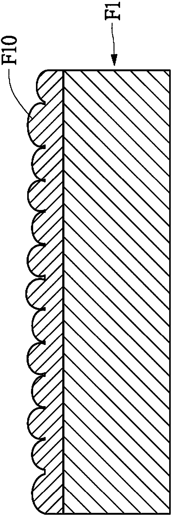
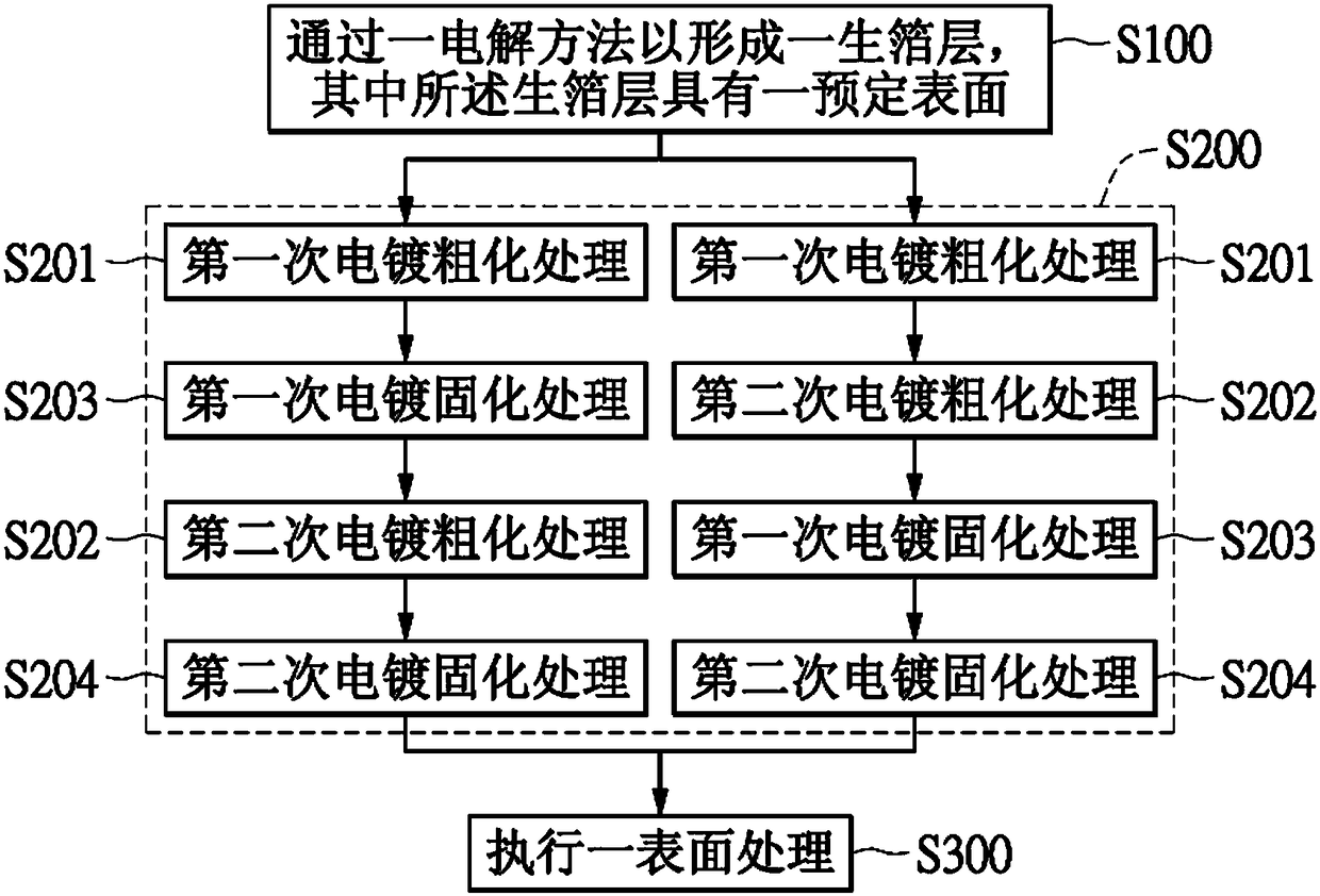
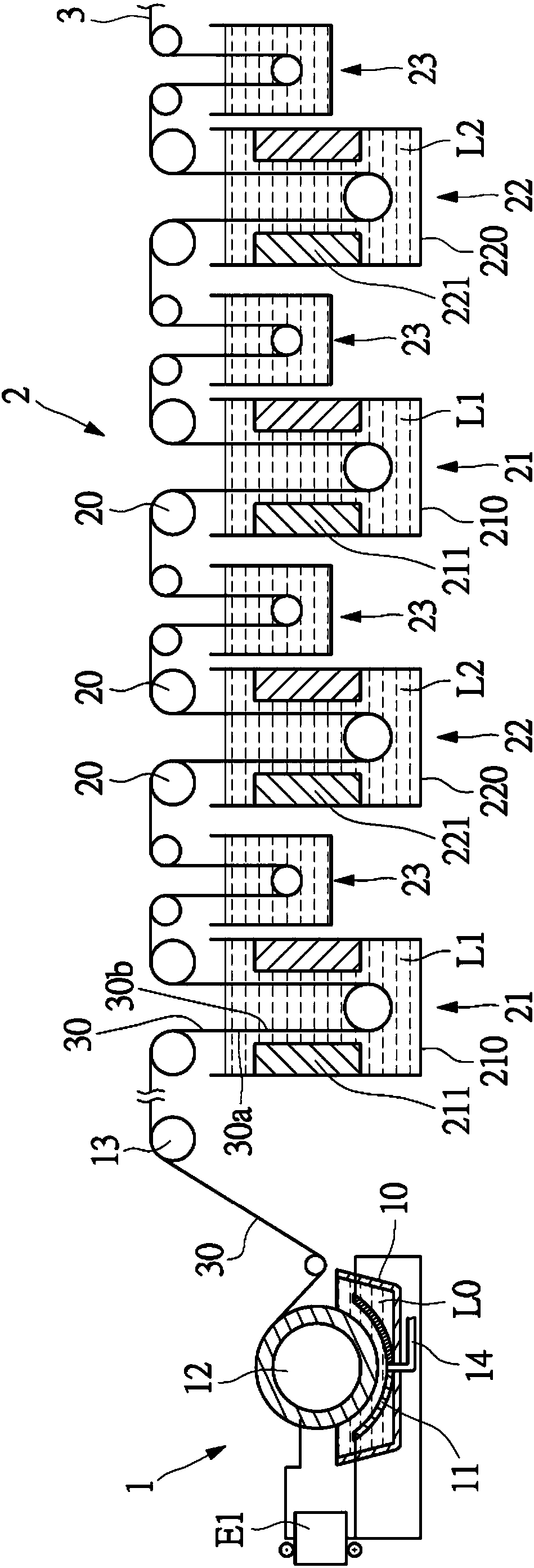
[0035] The following is an illustration of the implementation of the "method for manufacturing an electrolytic copper foil with approximately villous copper nodules and a circuit board assembly" disclosed by the present invention through specific examples. The manufacturing method provided by the embodiment of the present invention can obtain an electrodeposited copper foil with approximately villous copper nodules, which has low roughness and high peel strength. In addition, the circuit board assembly formed by bonding the electrodeposited copper foil with the approximate villi-shaped copper nodules and the resin substrate to each other can be applied to high-frequency signal transmission. Please refer to figure 2 and image 3 . figure 2 A flow chart showing a method for manufacturing an electrodeposited copper foil with approximate villous copper nodules according to an embodiment of the present invention, image 3 for execution figure 2 Schematic diagram of the equip...


PUM


Abstract

The invention discloses manufacturing methods of an electrolytic copper foil and circuit board assembly. The manufacturing methods of an electrolytic copper foil having needle-shaped particles includeforming a copper foil by an electrolyzing process, wherein the foil layer has a predetermined surface. Then, a surface treatment layer is formed on the predetermined surface of the copper foil to form an electrolytic copper foil having a needle-shaped structure on a surface layer. The surface treatment layer includes a plurality of needle-shaped copper particles, and a needle-shaped arrangement space exists between two adjacent needle-shaped copper particles. The steps of forming the surface treatment layer further includes performing a first electrolytic roughening treatment and a first electrolytic curing treatment, in which a first electrolyte solution used in the first electrolytic roughening treatment includes copper ions, sulfuric acid, arsenic trioxide, and tungstate ions, in whichthe copper concentration ranges from 3 to 40 g/L, the sulfuric acid concentration ranges from 100 to 120 g/L, the arsenic trioxide concentration is not more than 20 ppm, and the tungstate ion concentration ranges from 5 to 20 ppm. Thus, since the surface layer has the electrolyte copper foil having the needle-shaped structure and has a larger contact area with a resin substrate, higher peeling strength can be achieved.

Description

technical field [0001] The present invention relates to a method for manufacturing electrolytic copper foil and a circuit board assembly, in particular to a method for manufacturing an electrolytic copper foil with a fluffy structure on the surface, and a circuit board assembly using an electrolytic copper foil with a fluffy structure on the surface Production method. Background technique [0002] The existing copper foil used in printed circuit boards will be electroplated on the cathode wheel to form the original foil, and then undergo a post-processing process to form the final product. Post-processing includes roughening the rough surface of the original foil to form multiple copper nodules on the rough surface of the original foil, thereby increasing the bonding strength between the copper foil and the circuit substrate, that is, increasing the peel strength of the copper foil. [0003] However, electronic products tend to be high-frequency and high-speed in recent yea...

Claims


Application Information

Patent Timeline
IPC IPC(8): C25D7/06C25D3/38C25D5/10C25D5/48C25D5/56
CPCC01P2004/03C25D3/38C25D5/10C25D5/48C25D5/56C25D7/0614
Inventor 陈黼泽邹明仁林士晴
Owner NANYA PLASTICS CORP
Why Eureka
Try Eureka