
BZO glass and preparation method, as well as QLED device and manufacturing method

A glass and device technology, which is applied in the field of BZO glass and its preparation, QLED devices and its preparation, can solve the problems of short circuit, lower photoelectric performance of QLED devices, and poor uniformity of film thickness, etc., so as to improve uniformity, reduce trapping centers, and reduce defects Effect

Inactive Publication Date: 2018-09-14
TCL CORPORATION
View PDF3 Cites 0 Cited by
  • Summary
  • Abstract
  • Description
  • Claims
  • Application Information

AI Technical Summary

Problems solved by technology

[0005] In view of the above-mentioned deficiencies in the prior art, the object of the present invention is to provide a BZO glass and its preparation method, QLED device and its preparation method, aiming to solve the problem that many spikes will appear on the surface of the BZO film prepared by the existing method, resulting in the thickness of the subsequent film. Poor uniformity, spikes piercing the thin layer to cause a short circuit, forming defects at the interface between the spike and the adjacent thin layer, trapping carriers, and reducing the photoelectric performance of QLED devices

Method used


Image

  • BZO glass and preparation method, as well as QLED device and manufacturing method
  • BZO glass and preparation method, as well as QLED device and manufacturing method
  • BZO glass and preparation method, as well as QLED device and manufacturing method

Examples


Embodiment 1

[0062] A glass substrate with an area of ​​1.1m×1.3m×3mm is used, and an aqueous cleaning agent is added to spray the upper and lower surfaces of the glass. After scrubbing with a brush, enter the high-pressure spray ultrapure water to rinse the residual liquid on the glass surface, and finally pass through an 80°C wind Dry it in the knife chamber and send it to the LPCVD process.

[0063] The cleaned glass is rapidly heated to 155°C in the heating chamber and sent to the LPCVD reaction chamber, and the process pressure is adjusted to 5×10 -3 mbar, H 2 O / DEZ flow ratio is 1.1, DEZ / B 2 h 6 Flow ratio is 3, DEZ flow is 480sccm, H 2 O flow 528sccm, B 2 h 6 The flow rate is 160sccm, and the deposition time is 300s. The thickness of the BZO film is 1820nm, the sheet resistance is about 16Ω / □, and the haze is 25%. After the deposition is completed, it is sent to be corroded with a dilute HCl solution. The volume concentration of the dilute HCl solution is 0.5%, the solution t...

Embodiment 2

[0065] A glass substrate with an area of ​​1.1m×1.3m×3mm is used, and an aqueous cleaning agent is added to spray the upper and lower surfaces of the glass. After scrubbing with a brush, enter the high-pressure spray ultrapure water to rinse the residual liquid on the glass surface, and finally pass through an 80°C wind Dry it in the knife chamber and send it to the LPCVD process.

[0066] The cleaned glass is rapidly heated to 155°C in the heating chamber and sent to the LPCVD reaction chamber, and the process pressure is adjusted to 5×10 -3 mbar, H 2 O / DEZ flow ratio is 1.1, DEZ / B 2 h 6 Flow ratio is 3, DEZ flow is 480sccm, H 2 O flow 528sccm, B 2 h 6 The flow rate is 160sccm, and the deposition time is 300s. The thickness of the BZO film is 1820nm, the sheet resistance is about 16Ω / □, and the haze is 25%. After the deposition is completed, it is sent to be corroded with a dilute HCl solution. The volume concentration of the dilute HCl solution is 2%, the solution tem...

Embodiment 3

[0068] A glass substrate with an area of ​​1.1m×1.3m×3mm is used, and an aqueous cleaning agent is added to spray the upper and lower surfaces of the glass. After scrubbing with a brush, enter the high-pressure spray ultrapure water to rinse the residual liquid on the glass surface, and finally pass through an 80°C wind Dry it in the knife chamber and send it to the LPCVD process.

[0069] The cleaned glass is rapidly heated to 155°C in the heating chamber and sent to the LPCVD reaction chamber, and the process pressure is adjusted to 5×10 -3 mbar, H 2 O / DEZ flow ratio is 1.1, DEZ / B 2 h 6 Flow ratio is 3, DEZ flow is 480sccm, H 2 O flow 528sccm, B 2 h 6 The flow rate is 160sccm, and the deposition time is 300s. The thickness of the BZO film is 1820nm, the sheet resistance is about 16Ω / □, and the haze is 25%. After the deposition is completed, it is sent to be corroded with a dilute HCl solution. The volume concentration of the dilute HCl solution is 5%, the solution tem...


PUM

PropertyMeasurementUnit
thicknessaaaaaaaaaa
thicknessaaaaaaaaaa
thicknessaaaaaaaaaa

Abstract

The invention discloses a BZO glass and a preparation method, as well as a QLED device and a manufacturing method. The preparation method of the BZO glass comprises the following steps: A, preparing BZO glass; B, corroding a BZO film in the BZO glass through an acidic solution; C, cutting the BZO glass processed in step B to obtain the BZO glass with a required size. According to the preparation method of the BZO glass, the BZO film is deposited according to a chemical vapor deposition method, and then the BZO film is corroded through the acidic solution, thus burrs on the surface of the filmcan be relieved, and as a result, the uniformity of the thickness of the film in following process can be improved, and the problem that the burrs pierce a thin layer to cause short circuit is solved;the defects caused by the burrs and adjacent thin layer interface is reduced; carrier catching centers are decreased, and thus the purpose of improving the photoelectric performance of the QLED device can be improved.

Description

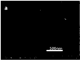
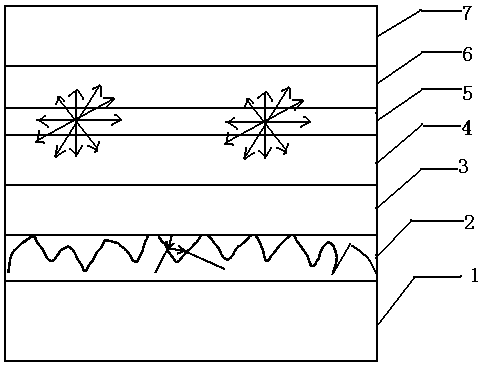
technical field [0001] The invention relates to the technical field of light-emitting diodes, in particular to a BZO glass and a preparation method, a QLED device and a preparation method. Background technique [0002] Due to the loss of the waveguide effect, most of the light can only propagate inside the QLED device and be absorbed, and the external quantum efficiency of traditional LED devices remains at 20%. Recently, there have been many improved technologies for the internal and external structures of QLED devices to improve the light extraction efficiency of QLED devices, such as scattering media, microscopic mirror arrays, nanoholes, and nanostructures. [0003] At present, in order to improve the light extraction efficiency of QLED devices, it is reported that BZO (boron-doped ZnO) glass is used to replace traditional ITO glass. The advantages are: 1) BZO has a microscopic and nano-light trapping structure, such as figure 1 2) Compared with ITO glass, the cost of B...

Claims


Application Information

Patent Timeline
Patent Type & Authority Applications(China)
IPC IPC(8): C03C17/245C03C15/00H01L51/52H01L51/56
CPCC03C15/00C03C17/245C03C2217/216C03C2217/24H10K50/80H10K71/00
Inventor 张东华向超宇李乐辛征航张滔
Owner TCL CORPORATION
Learn More