Preparation method for gallium doped polycrystalline silicon ingot and gallium doped polycrystalline silicon ingot

A technology of polycrystalline silicon ingots and polycrystalline silicon, which is applied in the preparation of gallium-doped polycrystalline silicon ingots and in the field of gallium-doped polycrystalline silicon ingots, which can solve the problems of uneven distribution of doping concentration and achieve uniform doping concentration

Inactive Publication Date: 2018-09-14
YINGLI ENERGY CHINA
View PDF4 Cites 7 Cited by
  • Summary
  • Abstract
  • Description
  • Claims
  • Application Information

AI Technical Summary

Problems solved by technology

[0003] In view of this, an embodiment of the present invention provides a method for preparing a gallium-doped polysilicon ingot and a gallium-doped polysilicon ingot to solve the problem of uneven doping concentration distribution of gallium in the prior art when preparing a gallium-doped polysilicon ingot

Method used


Image

  • Preparation method for gallium doped polycrystalline silicon ingot and gallium doped polycrystalline silicon ingot

Examples


Embodiment 1

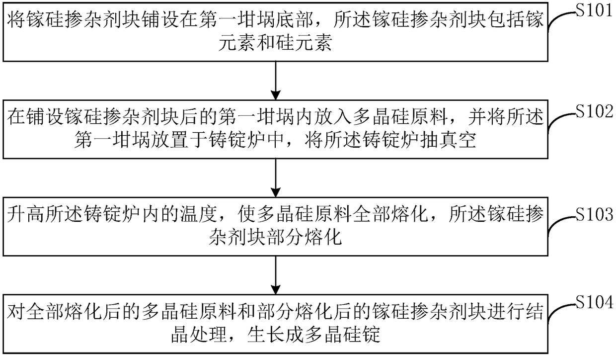
[0042] Please refer to figure 1 , the preparation method of gallium-doped polycrystalline silicon ingot comprises:

[0043] Step S101 , laying a gallium-silicon dopant block on the bottom of the first crucible, the gallium-silicon dopant block including gallium element and silicon element.

[0044] In the embodiment of the present invention, a plurality of SiGa dopant blocks are spread on the bottom of the first crucible so that the SiGa dopant blocks just cover the bottom of the crucible. The gallium silicon dopant block has a side length of 152 mm to 160 mm and a thickness of 10 mm to 20 mm. For example, if 36 gallium-silicon dopant blocks are laid flat on the bottom of a G6 crucible and placed in a single layer, the 36 gallium-silicon dopant blocks can just cover the bottom of the crucible.

[0045] Optionally, the mass ratio of silicon element to gallium element in the gallium-silicon dopant block is 100000:7 to 10000:35.

[0046] In the embodiment of the present invent...

Embodiment 2

[0072] A gallium-doped polycrystalline silicon ingot is prepared according to the preparation method of the gallium-doped polycrystalline silicon ingot described in the first aspect of the embodiment of the present invention, and has the beneficial effects of the first embodiment of the present invention.


PUM

PropertyMeasurementUnit
thicknessaaaaaaaaaa

Abstract

The invention is suitable for the technical field of photovoltaic cells, and provides a preparation method for a gallium doped polycrystalline silicon ingot and the gallium doped polycrystalline silicon ingot. The method comprises the following steps: spreading a gallium-silicon doping agent block on the bottom of a first crucible, wherein the gallium-silicon doping agent block comprises an element gallium and an element silicon; putting a polycrystalline silicon raw material into the first crucible which is layed with the gallium-silicon doping agent block, putting the first crucible into a cast ingot furnace, and performing vacuum-pumping on the cast ingot furnace; rising the temperature in the cast ingot furnace, completely melting the polycrystalline silicon raw material, and partiallymelting the polycrystalline silicon doping agent; and performing crystallization treatment on the completely-molten polycrystalline silicon raw material and the partially molten gallium-silicon doping agent block to grow to be the polycrystalline silicon ingot. The preparation method can be used for preparing the gallium doped polycrystalline silicon ingot with uniform doping concentration.

Description

technical field [0001] The invention belongs to the technical field of photovoltaic cells, and in particular relates to a preparation method of a gallium-doped polycrystalline silicon ingot and a gallium-doped polycrystalline silicon ingot. Background technique [0002] The silicon wafers for the production of polycrystalline silicon solar cells are processed from polycrystalline silicon ingots. Usually, polycrystalline silicon ingots are prepared by doping boron (B) to prepare p-type solar cell silicon wafers. However, when solar cells are working, B and the residual oxygen in the silicon wafers (O) will form a B-O complex under light, and form a B-Fe pair with the impurity iron (Fe) in the silicon wafer, which will cause attenuation of the solar cell and reduce the conversion efficiency of the solar cell. At present, the commonly used method is to dope gallium (Ga) into polycrystalline silicon ingots. However, the segregation coefficient of Ga in silicon liquid is very sma...

Claims


Application Information

Patent Timeline
Patent Type & Authority Applications(China)
IPC IPC(8): C30B28/06C30B29/06
CPCC30B28/06C30B29/06
Inventor 王坤潘家明王丙宽刘志强周秉林潘明翠
Owner YINGLI ENERGY CHINA
Why Eureka
Try Eureka