

Slide for powder with poor electric conductivity for SEM (scanning electron microscopes) and method for applying slide
A technology of conductive performance and object slide, which is applied in the direction of material analysis, measurement device, instrument, etc. using wave/particle radiation, which can solve the problem that the conductive film cannot completely cover the powder particles, contaminate the optical path system of the electrode shoe of the electron microscope, and the powder cannot produce electrical conductivity. problems such as access, to achieve the effect of improving the economic performance of the experiment, reducing the time of gold spraying, and easy to spray gold.
- Summary
- Abstract
- Description
- Claims
- Application Information
AI Technical Summary
Problems solved by technology
Method used
Image

Examples
Embodiment 1
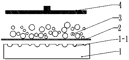
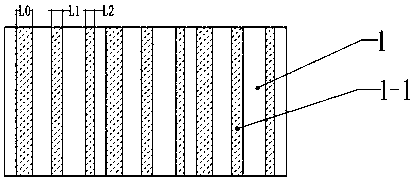
[0026] Firstly, the material of the slide 1 is selected as 45 steel, and then it is machined into 20mm×10mm×4mm. And use ion etching equipment to subtractively process it into an arc-shaped groove 1-1 that can accommodate particles, such as figure 1 As shown, the arc-shaped trench sizes L0, L1, and L2 are etched with widths of 300 μm, 10 μm, and 50 nm, such as figure 2 shown.
[0027] Next, clean the surface of the slide with anhydrous alcohol to remove impurities such as oil on the surface, dry it, and then stick the conductive adhesive 2 on the slide to ensure that the conductive glue covers the arc groove on the surface of the slide.
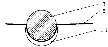
[0028] Further, sprinkle the dispersed WC ceramic powder particles 3 on the conductive adhesive, then use a blower to blow off the particles that are not firmly adhered, and then press them with a glass sheet 4 to ensure that the particles on the groove can be pressed into the groove by the glass sheet. Groove 1-1, wherein the conductive g...
Embodiment 2
[0031] Firstly, the material of the slide 1 is selected as TC4 alloy, and then it is machined into 20mm×10mm×4mm. And use ion etching equipment to subtractively process it into a square groove 1-1 that can accommodate particles, such as Figure 4 As shown, the dimensions L0, L1, and L2 of the square groove are etched with widths of 1000 μm, 50 μm, and 100 nm, such as Figure 5 shown.
[0032] Next, the surface of the slide is cleaned and dried, and then the conductive glue 2 is stuck on the slide to ensure that the conductive glue covers the square groove on the surface of the slide.
[0033] Further, sprinkle the dispersed Al on the conductive adhesive 2 o 3 Ceramic powder particles 3, then use a blower to blow off the particles that are not firmly adhered, and then press them with a glass sheet 4 to ensure that the particles on the groove can be pressed into the groove 1-1 by the glass sheet, wherein the conductive adhesive 2 is in the groove 1-1. Between the pressed par...
Embodiment 3
[0036] First, the material of the slide 1 is selected as brass H90 alloy, and then machined into a size of 20mm×10mm×4mm. And use additive equipment to process it into a metal mesh 1-2 and form a groove 1-1 that can accommodate particles, such as Figure 7 As shown, the metal mesh gap width D0 is 500μm, such as Figure 8 shown.
[0037] Next, the surface of the slide is cleaned and dried, and then the conductive glue 2 is stuck on the slide to ensure that the conductive glue covers the polygonal groove on the surface of the slide.
[0038] Further, sprinkle the dispersed Al on the conductive adhesive 2 o 3 Powder particles 3, then use a blower to blow off the particles that are not firmly adhered, and then press them with a glass sheet 4 to ensure that the particles on the groove can be pressed into the groove 1-1 by the glass sheet, in which the conductive adhesive 2 is being pressed The particle 3 is in the middle of the groove 1-1. Finally remove the glass sheet 4 to p...
PUM
| Property | Measurement | Unit |
|---|---|---|
| width | aaaaa | aaaaa |
| width | aaaaa | aaaaa |
Abstract
Description
Claims
Application Information