Microstrip antenna based on artificial magnetic conductor

A technology of artificial magnetic conductors and microstrip antennas, which is applied to the structural forms of antennas, electrical components, and radiation elements, etc., can solve the problems of microstrip antennas with complex structures, large sizes, return loss and gain effects that cannot meet technical requirements, etc. Achieve the effects of easy industrial processing, increased gain, and simple structure

Active Publication Date: 2018-09-14
NANJING UNIV OF POSTS & TELECOMM
View PDF7 Cites 9 Cited by
  • Summary
  • Abstract
  • Description
  • Claims
  • Application Information

AI Technical Summary

Problems solved by technology

However, the above-mentioned microstrip antennas are complex in structure and large in size, and the return loss and gain effects still cannot meet the technical requirements.

Method used


Image

  • Microstrip antenna based on artificial magnetic conductor
  • Microstrip antenna based on artificial magnetic conductor
  • Microstrip antenna based on artificial magnetic conductor

Examples


Embodiment 1

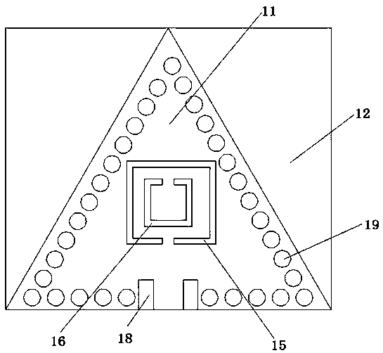
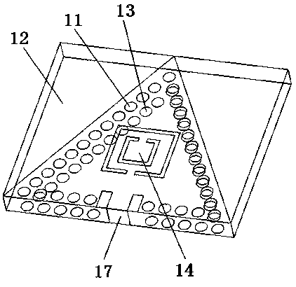
[0039] A microstrip antenna based on an artificial magnetic conductor, such as Figure 5As shown, it includes an isosceles triangular microstrip antenna and an artificial magnetic conductor reflection substrate, wherein the artificial magnetic conductor reflection unit adopts a Rogers 6010 dielectric substrate with a dielectric constant of 10.2 and a thickness of 1.0mm. Image 6 It is the S parameter simulation waveform diagram of this embodiment, as can be seen from the figure, the center frequency of this embodiment is 12.3GHz, the return loss is greater than 12dB, the antenna gain is 4.9dB, and the working performance is good; Figure 8 It is the 3D radiation pattern of this embodiment, indicating the spatial distribution of the electric field, the color depth represents the radiation intensity, the darker the color, the stronger the electric field, and the lighter the color, the weaker the electric field).

Embodiment 2

[0041] A microstrip antenna based on an artificial magnetic conductor, such as Figure 5 As shown, the artificial magnetic conductor reflection unit adopts a Rogers 5880 dielectric substrate with a dielectric constant of 2.2 and a thickness of 1.0mm. Figure 7 It is the S-parameter simulation waveform diagram of this embodiment, as can be seen from the figure, the center frequency is 12.3GHz, the return loss is greater than 14dB, the antenna gain is 7.8dB, and the working performance is good; Figure 9 is the 3D radiation pattern of this example, compared to Figure 8 , the radiation direction of this embodiment is changed from bidirectional to unidirectional, the gain is increased by nearly 3dB, the directivity becomes better, and the high gain of the antenna is realized.

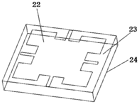
[0042] In the present invention, a triangular microstrip antenna with high radiation rate and an artificial magnetic conductor reflective substrate with the same phase reflection characteristics are combi...


PUM


Abstract

The invention provides a microstrip antenna based on an artificial magnetic conductor. The microstrip antenna comprises a triangular microstrip antenna and an artificial magnetic conductor reflectionsubstrate, and the triangular microstrip antenna is arranged in a position 0.1mm over a central position of the artificial magnetic conductor reflection substrate by being supported by a non-metal insulated column; the triangular microstrip antenna comprises a triangular radiation patch, a dielectric layer and a grounding plate arranged sequentially from top to bottom, the shape and size of the grounding plate correspond to those of the triangular radiation patch respectively, a complementary resonant ring structure is etched in a central position of the triangular radiation patch, a coplanarwaveguide feed point is arranged in the central point position of the bottom side of the triangular radiation patch, and the edge of the triangular radiation patch is provided with air vents penetrating the antenna at equal interval except the feed point; and the artificial magnetic conductor reflection substrate is formed by splicing artificial magnetic conductor reflection units arranged in a 3*3 array, and the shape and size of the artificial magnetic conductor reflection unit correspond to those of the dielectric layer respectively. The microstrip antenna is simple in structure, easy to process and characterized by being mini and high in gain.

Description

technical field [0001] The invention relates to a microstrip antenna, in particular to a microstrip antenna based on an artificial magnetic conductor, and belongs to the technical field of millimeter waves. Background technique [0002] In recent years, artificial magnetic conductors (Artificial Magnetic Conductors, AMC) have become one of the research hotspots in the field of microwave and millimeter waves. Artificial magnetic conductors, also known as high-impedance surfaces, have in-phase reflection characteristics and are widely used in the design of waveguides, antennas, and thin absorbers. Traditional artificial magnetic conductor structures include the mushroom-shaped electromagnetic bandgap (EBG) structure proposed by Sievenpiper and the photonic bandgap (PBG) structure proposed by Itoh, which can be effectively However, due to the presence of metal vias in the mushroom-type EBG structure, the fabrication is more complicated and the processing cost is higher. Althou...

Claims


Application Information

Patent Timeline
Patent Type & Authority Applications(China)
IPC IPC(8): H01Q1/38H01Q13/08H01Q19/10
CPCH01Q1/38H01Q13/08H01Q19/10
Inventor 许锋刘寅初江涛
Owner NANJING UNIV OF POSTS & TELECOMM
Why Eureka
Try Eureka