

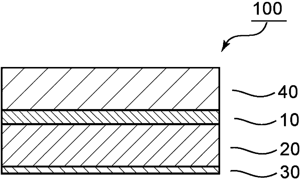
Optical laminate and image display device in which said optical laminate is used
A technology of optical laminates and protective layers, which is applied in optics, optical components, nonlinear optics, etc., can solve problems such as deviations in optical characteristics, and achieve the effects of excellent display characteristics and excellent anti-reflection functions
- Summary
- Abstract
- Description
- Claims
- Application Information
AI Technical Summary
Problems solved by technology
Method used
Image

Examples
Embodiment
[0138] Hereinafter, although an Example demonstrates this invention concretely, this invention is not limited to these Examples. In addition, the measurement method of each characteristic is as follows.
[0139] (1) Thickness
[0140] The conductive layer was measured by an interference film thickness measurement method using MCPD2000 manufactured by Otsuka Electronics. For other films, measurement was performed using a digital micrometer (KC-351C manufactured by Anritsu Corporation).
[0141] (2) The phase difference value of the phase difference layer
[0142] The refractive indices nx, ny, and nz of the retardation layer (retardation film) used in Examples and Comparative Examples were measured with an automatic birefringence measurement device (manufactured by Oji Scientific Instruments, Ltd., automatic birefringence meter KOBRA-WPR). . The measurement wavelength of the in-plane retardation Re was 450 nm and 550 nm, the measurement wavelength of the thickness direction...
Synthetic example 1
[0163] [Synthesis Example 1] Synthesis of bis[9-(2-phenoxycarbonylethyl)fluoren-9-yl]methane (BPFM)
[0164] Synthesis was carried out by the method described in JP 2015-25111.
Synthetic example 26
[0165] [Synthesis Example 2] Synthesis of 6,6'-dihydroxy-3,3,3',3'-tetramethyl-1,1'-spirobiindane (SBI)
[0166] Synthesis was carried out by the method described in JP 2014-114281.
[0167] [Synthesis example and characteristic evaluation of polycarbonate resin]
[0168] The abbreviations and the like of the compounds used in the following Examples and Comparative Examples are as follows.
[0169] BPFM: bis[9-(2-phenoxycarbonylethyl)fluoren-9-yl]methane
[0170] ・BCF: 9,9-bis(4-hydroxy-3-methylphenyl)fluorene (manufactured by Osaka Gas Chemicals Co., Ltd.)
[0171] ・BHEPF: 9,9-bis[4-(2-hydroxyethoxy)phenyl]fluorene (manufactured by Osaka Gas Chemicals Co., Ltd.)
[0172] · ISB: Isosorbide (manufactured by Roquette Freres, trade name: POLYSORB)
[0173] SBI: 6,6'-dihydroxy-3,3,3',3'-tetramethyl-1,1'-spirobiindane
[0174] ・SPG: spiroglycol (manufactured by Mitsubishi Gas Chemical Co., Ltd.)
[0175] ・PEG: polyethylene glycol number average molecular weight: 1000 (manufac...
PUM
| Property | Measurement | Unit |
|---|---|---|
| glass transition temperature | aaaaa | aaaaa |
| glass transition temperature | aaaaa | aaaaa |
| density | aaaaa | aaaaa |
Abstract
Description
Claims
Application Information