A double-layer vibration isolation structure and preparation method for vibration isolation of mems devices

A vibration isolation and device technology, which is applied in the field of double-layer vibration isolation structure and preparation, can solve the problems of complex active vibration isolation structure, difficult electronic compensation, and increased power consumption of devices, so as to make up for the lack of vibration isolation performance and improve economies of scale , Improve the effect of vibration isolation

Active Publication Date: 2019-12-31
HEFEI UNIV OF TECH
View PDF5 Cites 0 Cited by
  • Summary
  • Abstract
  • Description
  • Claims
  • Application Information

AI Technical Summary

Problems solved by technology

Output errors have a particularly large impact on high-Q and high-resonance MEMS devices such as gyroscopes and resonant sensors, because their internal low damping will amplify the influence of errors at the resonance frequency bandwidth, and it is difficult to conduct electronic testing due to the unpredictability of errors. compensate
3) The structure of the MEMS device is damaged
Although active vibration isolation has high vibration isolation accuracy; however, active vibration isolation is often difficult to achieve in complex structures and processes, and additional power supply is required to increase the power consumption of the device

Method used


Image

  • A double-layer vibration isolation structure and preparation method for vibration isolation of mems devices
  • A double-layer vibration isolation structure and preparation method for vibration isolation of mems devices
  • A double-layer vibration isolation structure and preparation method for vibration isolation of mems devices

Examples


Embodiment 1

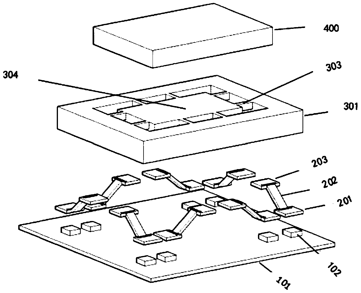
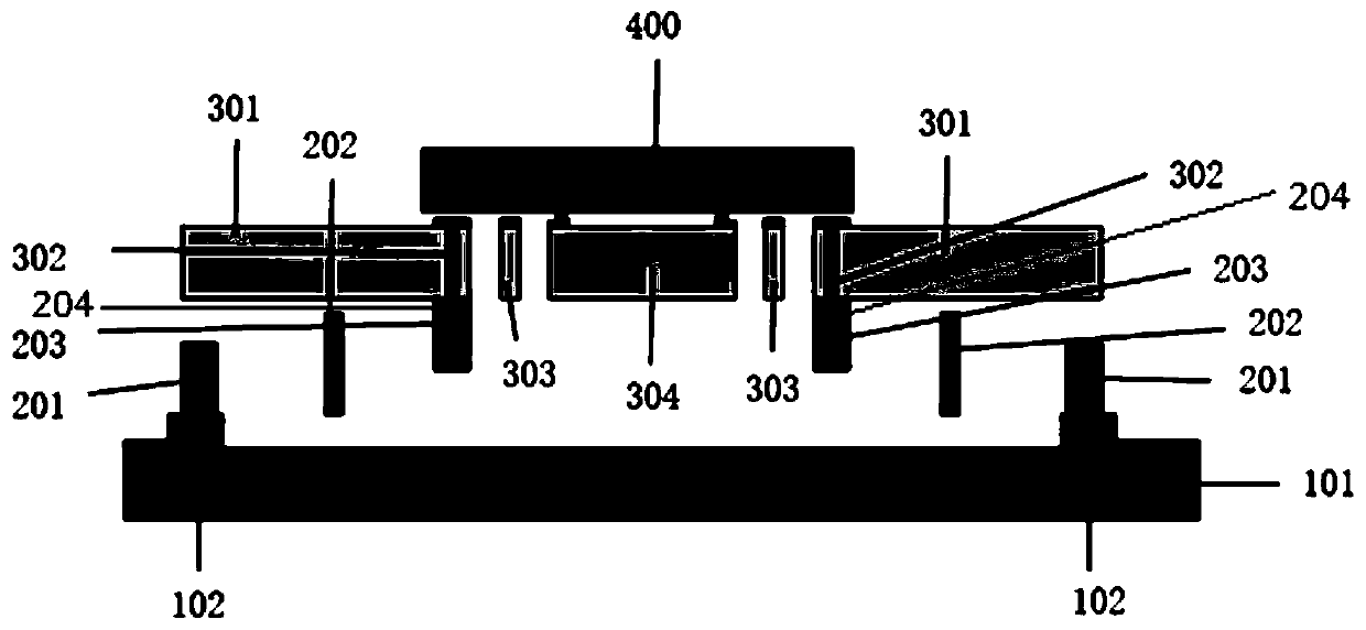
[0049] A double-layer vibration isolation structure for MEMS devices sequentially includes a first-layer vibration isolation system, a second-layer vibration isolation system, and a silicon substrate 101 from top to bottom;

[0050] Such as figure 1 combine figure 2 , Figure 4 As shown, the first layer of vibration isolation system includes a connection frame 301, a vibration isolation platform 304 and several vibration isolation beams 303; the connection frame 301 is surrounded by the vibration isolation platform 304, and several vibration isolation beams 303 are connected between the connection frame 301 and the vibration isolation platform 304; the connection frame 301 is provided with a first through hole 302 close to each vibration isolation beam 303, and a through hole lead is provided in the first through hole 302; an insulating layer is provided on the upper surface of the vibration isolation beam 303, and the insulating layer Metal leads are provided on the top; t...

Embodiment 2

[0069] The steps of preparing a double-layer vibration isolation structure for vibration isolation of MEMS devices are as follows:

[0070] (1) Prepare slices: prepare a 475 μm thick double-sided polished silicon substrate 305, a 500 μm thick glass slice 306, and a 500 μm thick silicon substrate 101;

[0071] (2) The first photolithography: such as Figure 5 As shown, the double-sided polished silicon substrate 305 is cleaned with deionized water, the cleaned double-sided polished silicon substrate 305 is spin-coated with a layer of photoresist, and the mask plate is used for inductively coupled plasma (ICP) etching , etch a shallow step with a height of 3-4 μm;

[0072] (3) Silicon glass bonding: such as Image 6 As shown, the side of the silicon substrate 305 etched in step 2 with a shallow step is bonded to the glass sheet 306 in step 1 by bonding technology;

[0073] (4) The second photolithography: if Figure 7 As shown, the upper pad 203, the second through hole 204,...


PUM


Abstract

The invention provides a double-layer vibration isolation structure for isolating vibration of an MEMS (micro-electromechanical systems) device and a method for preparing the double-layer vibration isolation structure. The double-layer vibration isolation structure sequentially comprises a first-layer vibration isolation system, a second-layer vibration isolation system and a silicon substrate from top to bottom. The MEMS device is welded above the first-layer vibration isolation system; the first-layer vibration isolation system comprises a connecting frame, a vibration isolation platform anda plurality of vibration isolation beams; the second-layer vibration isolation system comprises a plurality of vibration isolation assemblies, and each vibration isolation assembly comprises a lowerpad, a twisting beam and an upper pad which are sequentially connected with one another. The method for preparing the double-layer vibration isolation structure includes ten steps of sheet preparing,first photoetching, silica glass bonding, second photoetching, third photoetching, metal sputtering, through hole wire leading, fourth photoetching, substrate insulation layer and metal layer manufacturing and transient liquid phase diffusion bonding. The double-layer vibration isolation structure and the method have the advantages that the problem of insufficient vibration isolation performance during high-frequency vibration due to passive vibration isolation can be solved by the aid of the double-layer vibration isolation structure; the double-layer vibration isolation structure is simple,additional power sources can be omitted, and power consumption of the device can be reduced to a great extent.

Description

technical field [0001] The invention belongs to the technical field of MEMS, and in particular relates to a double-layer vibration isolation structure and a preparation method for vibration isolation of MEMS devices. Background technique [0002] MEMS is a micro-electromechanical device or system that integrates micromechanical and microelectronic functions. Devices based on MEMS technology (such as MEMS sensors and drivers) are small in size, light in weight, low in power consumption, good in durability, and low in price. It is widely used due to its stable performance and other advantages, especially in the automotive, aerospace and electronic industries. Many MEMS devices often need to work in harsh vibration environments. For example, MEMS sensors used in ordinary cars will withstand random vibration loads of 0-400 Hz for a long time, and MEMS devices used on spacecraft will withstand random vibrations of 20-2000 Hz during launch. load. The device will bear the random ...

Claims


Application Information

Patent Timeline
Patent Type & Authority Patents(China)
IPC IPC(8): B81B7/02B81B1/00B81B7/00B81C1/00
CPCB81B1/00B81B7/0032B81B7/02B81C1/00261B81C1/00333
Inventor 许高斌杨海洋马渊明陈兴徐枝蕃
Owner HEFEI UNIV OF TECH
Why Eureka
Try Eureka