
Nano metal substrate and manufacturing method for ultra-fine circuit fpc and cof materials

A nano-metal and ultra-fine line technology, applied in the direction of chemical instruments and methods, applications, household appliances, etc., to achieve the effects of size expansion and contraction, improvement of hardness and flame retardancy, and increase of adhesion

Active Publication Date: 2019-11-12
KUSN APLUS TEC CORP
View PDF8 Cites 0 Cited by
  • Summary
  • Abstract
  • Description
  • Claims
  • Application Information

AI Technical Summary

Problems solved by technology

[0007] The technical problem mainly solved by the present invention is to provide a nano-metal substrate and a manufacturing method for ultra-fine line FPC and COF materials, which have excellent ion migration resistance, dimensional stability, chemical resistance, heat resistance and high temperature resistance It is suitable for laser processing, suitable for laser processing of blind holes / micro holes, and is not easy to produce pinholes, suitable for thin line etching, and not easy to side etch; the invention adopts nano-copper design to meet the needs of the development of thin line substrates

Method used


Image

  • Nano metal substrate and manufacturing method for ultra-fine circuit fpc and cof materials
  • Nano metal substrate and manufacturing method for ultra-fine circuit fpc and cof materials
  • Nano metal substrate and manufacturing method for ultra-fine circuit fpc and cof materials

Examples


Embodiment

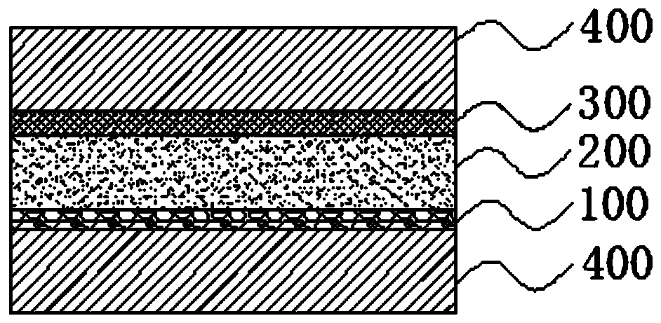
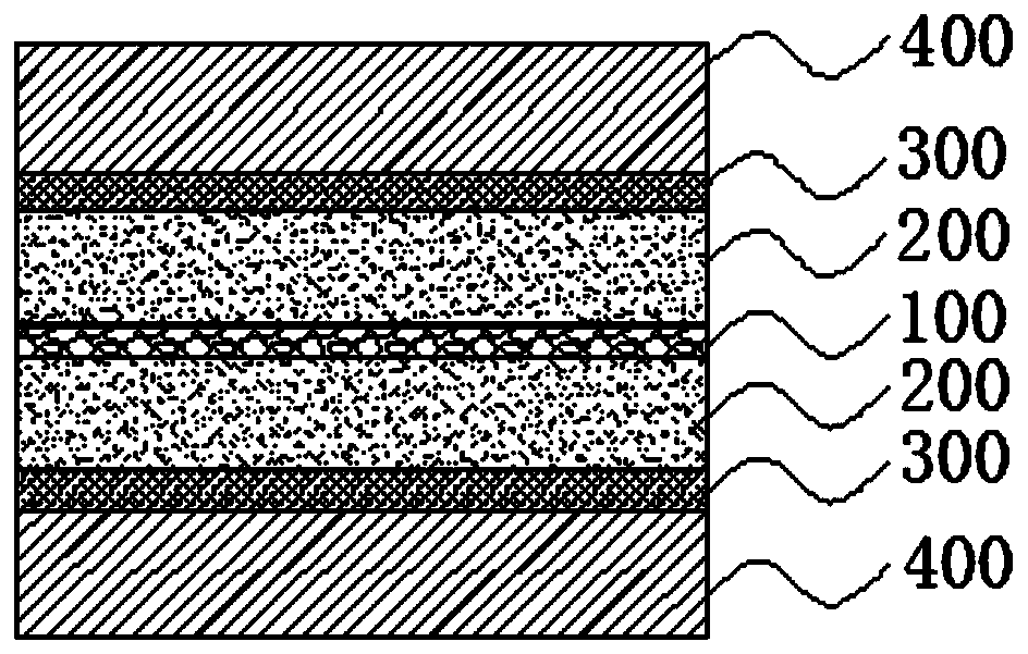
[0062] Embodiment: a kind of nanometer metal substrate that is used for ultrafine line FPC and COF material, as Figure 1-10 As shown, the present invention includes a low thermal expansion coefficient polyimide layer 100, a roughened polyimide layer 200 formed on at least one side of the low thermal expansion coefficient polyimide layer 100, and a roughened polyimide layer 200 formed on the roughened polyimide layer. The ultra-thin nano-metal layer 300 and the protective film layer 400 on the other side of the amine layer 200, the roughened polyimide layer 200 is interposed between the low thermal expansion coefficient polyimide layer 100 and the ultra-thin nano-metal layer 300 Between, the ultra-thin nano-metal layer 300 is between the roughened polyimide layer 200 and the protective film layer 400;

[0063] The thickness of the low thermal expansion coefficient polyimide layer 100 is 12.5-100um;

[0064] The thickness of the roughened polyimide layer 200 is 2-5um;

[0065...


PUM

PropertyMeasurementUnit
thicknessaaaaaaaaaa
surface roughnessaaaaaaaaaa
thicknessaaaaaaaaaa

Abstract

The invention discloses a nano-metal substrate for an ultrafine line FPC (Flexible Printed Circuit) and COF (Chip On Film) material and a manufacturing method. The nano-metal substrate comprises a polyimide layer with a low thermal expansion coefficient, a roughened polyimide layer formed on at least one side of the polyimide layer with a low thermal expansion coefficient, an ultra-thin nano-metallayer and a protective film layer formed on the other side of the roughened polyimide layer; the roughened polyimide layer is arranged between the polyimide layer with a low thermal expansion coefficient and the ultra-thin nano-metal layer; and the ultra-thin nano-metal layer is arranged between the roughened polyimide layer and the protective film layer. The nano-metal substrate is excellent inion migration resistance, dimensional stability, chemical resistance, heat resistance, high-temperature resistance and adhesion, suitable for laser processing blind holes / micropores, not easy to generate pinholes, suitable for fine line etching, and not easy to be etched. The invention adopts nano-copper design to meet the needs of thinning development of substrates.

Description

technical field [0001] The invention belongs to the technical field of electronic substrates, in particular to a nanometer metal substrate used for ultra-fine line FPC and COF materials. Background technique [0002] FPC (Flexible Printed Circuit), commonly known as "soft board", has the advantages of lightness, thinness, shortness, and smallness. It is widely used in small electronic products such as mobile phones, digital cameras, and digital cameras. COF ( ChipOn Film (chip-on-film packaging) technology is a technology that uses a flexible circuit board as a package chip carrier to combine the chip with the flexible circuit board circuit. As electronic products tend to be miniaturized, FPC or COF flexible circuit boards are required to be more powerful in function and tend to develop in the direction of high frequency, high density and thin lines. [0003] Flexible copper-clad laminates are substrate materials processed by FPC or COF, and the high-density and thin-line p...

Claims


Application Information

Patent Timeline
Patent Type & Authority Patents(China)
IPC IPC(8): B32B27/28B32B27/08B32B27/06B32B33/00B32B7/12
CPCB32B7/12B32B27/06B32B27/08B32B27/281B32B33/00B32B2307/306B32B2307/3065B32B2307/536B32B2307/734B32B2457/08
Inventor 林志铭李韦志李建辉
Owner KUSN APLUS TEC CORP
Learn More