Three-dimensional memory and manufacturing method thereof

A manufacturing method and memory technology, applied in the direction of electric solid-state devices, semiconductor devices, electrical components, etc., can solve the problems of inconsistent boss heights, insufficient energy injection, and inability to reach, so as to reduce growth defects, improve film quality, and improve reliability effect

Active Publication Date: 2018-10-09
YANGTZE MEMORY TECH CO LTD
View PDF5 Cites 6 Cited by
  • Summary
  • Abstract
  • Description
  • Claims
  • Application Information

AI Technical Summary

Problems solved by technology

[0005] However, in the actual manufacturing process, since the aspect ratio of the channel hole 2H is too large (for example, greater than or equal to 10, 20), it is very difficult to remove the defects at the bottom, and the film formation quality of the epitaxial growth boss 1E is not good, such as Figure 1b The mesas shown have inconsistent heights, voids at the bottom, or excessively large vertical channel layer growth defects caused by defects at the top of mesas 1E
In addition, during the ion implantation doping process, because the aspect ratio of the channel hole 2H is too large, the ion implantation range is relatively long. If the verticality of the implantation process is not well controlled, a considerable part of the ions will be incident on the stacked structure 2 On the sidewall, thus affecting the etching selectivity between the sub-layers of the stacked structure 2, so that the active region of the bottom selection transistor deviates from the designed layout, or cannot reach the boss at the bottom of the channel hole 2H due to insufficient implantation energy 1E

Method used


Image

  • Three-dimensional memory and manufacturing method thereof
  • Three-dimensional memory and manufacturing method thereof
  • Three-dimensional memory and manufacturing method thereof

Examples


Embodiment Construction

[0049] The features and technical effects of the technical solution of the present invention will be described in detail below with reference to the accompanying drawings and in conjunction with schematic embodiments, and a new three-dimensional memory manufacturing method that can effectively improve the film formation quality of the channel region of a 3D NAND memory device is disclosed. It should be pointed out that similar reference numerals represent similar structures, and the terms "first", "second", "upper", "lower" and the like used in this application can be used to modify various device structures. These modifications do not imply a spatial, sequential or hierarchical relationship of the modified device structures unless specifically stated.

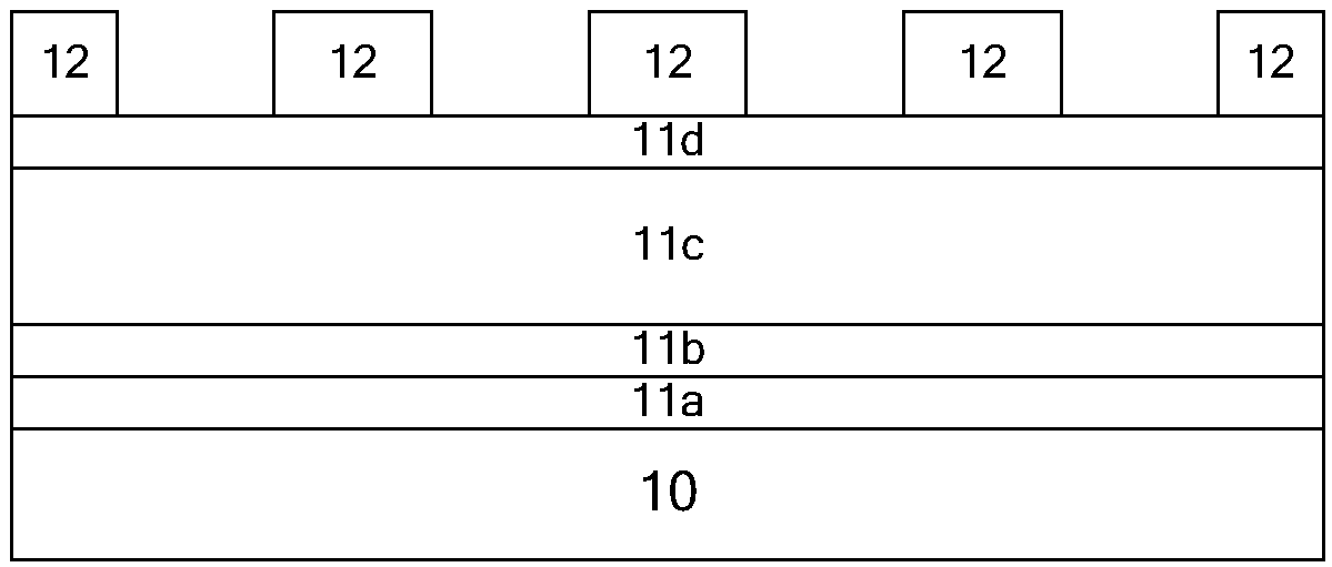
[0050] like image 3 As shown, a schematic flowchart of a method for manufacturing a three-dimensional memory according to an embodiment of the present invention is described. Firstly, a hard mask is formed on the substrate and...


PUM


Abstract

The invention discloses a three-dimensional memory and a manufacturing method thereof. The manufacturing method comprises the steps of forming a hard mask layer on a substrate and performing patterning; forming a semiconductor lug boss on the substrate through a hard mask pattern; forming a doped region on the top of the semiconductor lug boss; forming dielectric layer stack on the hard mask pattern and the semiconductor lug boss; and performing etching on the dielectric layer stack to form a perpendicular channel hole for exposing the semiconductor lug boss. By virtue of the manufacturing method of the three-dimensional memory disclosed in the invention, the doped lug boss is formed on the substrate firstly by the hard mask pattern, and then the channel hole is formed in the dielectric layer stack, so that the film forming quality, height and doping concentration uniformity of the lug boss at the bottom of the channel hole can be improved, the growth defects of the perpendicular channel region is lowered, and device reliability is improved.

Description

technical field [0001] The invention relates to a three-dimensional memory and a manufacturing method thereof, in particular to a three-dimensional NAND memory unit transistor and a manufacturing method thereof. Background technique [0002] In order to improve the density of memory devices, the industry has made extensive efforts to develop methods of reducing the size of two-dimensionally arranged memory cells. As the size of memory cells in two-dimensional (2D) memory devices continues to shrink, signal collisions and interference can increase significantly, making it difficult to perform multi-level cell (MLC) operations. In order to overcome the limitations of 2D memory devices, the industry has developed memory devices with a three-dimensional (3D) structure to increase integration density by three-dimensionally arranging memory cells on a substrate. [0003] A typical 3D NAND manufacturing process such as Figure 1a As shown, a stacked structure 2 (for example, a str...

Claims


Application Information

Patent Timeline
IPC IPC(8): H01L27/11524H01L27/11556H01L27/1157H01L27/11582
CPCH10B41/35H10B41/27H10B43/35H10B43/27
Inventor 刘隆冬王猛
Owner YANGTZE MEMORY TECH CO LTD
Why Eureka
Try Eureka