Analysis method for submillimeter-scale defects on the surface of coating materials

A sub-millimeter-level defect analysis technology, which is applied in the direction of material analysis, material analysis, and optical testing of defects/defects using wave/particle radiation. Small problems, to achieve the effect of improving surface quality

Active Publication Date: 2020-09-04
武汉钢铁有限公司
View PDF4 Cites 0 Cited by
  • Summary
  • Abstract
  • Description
  • Claims
  • Application Information

AI Technical Summary

Problems solved by technology

However, there are great difficulties in the preparation of cross-sectional samples with submillimeter defects. Due to the small size of the defects, the preparation is easy to cause damage to the defects and the patterned coating (over-grinding removes the defects, and grinding causes the destruction of the patterned coating. Introduce external interference, etc.), and this damage is irreversible, which will cause analysis failure, so it is particularly difficult to analyze by traditional preparation methods
The FIB / SEM dual-beam system can use focused ion beams to cut and analyze micron-level defects. However, due to the small effective area of ​​ion beam cutting, it has a better analysis effect on defects with a size of several microns and tens of microns. Analysis of submillimeter defects is limited and the equipment is expensive
[0005] However, when the chemical reagent corrosion method is used to remove the surface coating for analysis, due to the different properties of the surface coating, each coating or coating requires a different corrosion medium. Some coatings have good corrosion resistance, and it is difficult to pass the corrosion method. At the same time, the corrosion method may destroy the effective information in the defect, especially for small-sized defects, the corrosion method is difficult to control the corrosion rate and corrosion degree, and the effective information obtained is less, and the corrosion method may also cause sample surface contamination and environmental pollution

Method used


Image

  • Analysis method for submillimeter-scale defects on the surface of coating materials
  • Analysis method for submillimeter-scale defects on the surface of coating materials
  • Analysis method for submillimeter-scale defects on the surface of coating materials

Examples


Embodiment Construction

[0036] The present invention will be further described in detail below in conjunction with the accompanying drawings and specific embodiments, so as to facilitate a clearer understanding of the present invention, but they do not limit the present invention.

[0037] A method for analyzing submillimeter defects on the surface of a coating material, comprising the steps of:

[0038] 1) Sample preparation and macroscopic observation

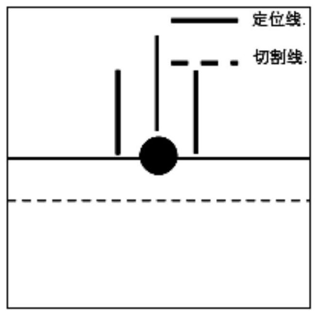
[0039] 1a) Sample preparation: centering on the defect, cut the sample to be analyzed into a sample of 20mm×20mm×thickness (≤10mm). If the size of the sample to be analyzed is small, no cutting is required;

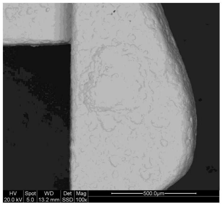
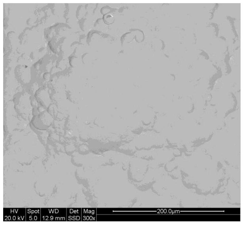
[0040] 1b) Macroscopic observation: After the sample is placed in an alcohol solution for ultrasonic cleaning, use an optical microscope to observe and take pictures of submicron defects on the coating surface of the sample map, and record the optical features of the defect, such as length, width, Whether the surface is convex or concave, etc....


PUM

PropertyMeasurementUnit
thicknessaaaaaaaaaa
thicknessaaaaaaaaaa

Abstract

The invention discloses a method for analyzing submillimeter-scale defects on the surface of a coated material. The method comprises macroscopic observation, section sample preparation, polishing andcomprehensive analysis. The limitation on defect size by section sample preparation in traditional defect analysis is broken through, section samples with submillimeter-scale surfaces are prepared andanalyzed under the condition that surface coated layers are not removed by aid of an FIB / SEM double-beam system or with a chemical method, effective information of samples is reserved, and the problem about section sample preparation in the coated surface submillimeter-scale defect analysis is effectively solved.

Description

technical field [0001] The invention belongs to the technical field of material surface quality analysis, and specifically refers to a method for analyzing submillimeter defects on the surface of coating materials. Background technique [0002] Coating refers to the formation of a covering layer on the surface of the material by physical or chemical methods, thereby improving the appearance of the material, or improving the mechanical or corrosion resistance of the surface. However, due to surface quality problems of raw materials or fluctuations in the manufacturing process, defects are prone to occur on the surface of the coating, which in turn affects the end-use performance of the material. With the improvement of manufacturing technology and the appearance of some precision coated parts, the defects on the surface of coated materials are developing in the direction of miniaturization, gradually developing from centimeter and millimeter levels to sub-millimeter levels. H...

Claims


Application Information

Patent Timeline
Patent Type & Authority Patents(China)
IPC IPC(8): G01N23/2206G01N23/2251G01N23/203G01N23/2273G01N23/20008G01N21/95
CPCG01N21/95G01N23/20008G01N23/203G01N23/2202G01N23/2206G01N23/2251G01N23/2273G01N2223/045G01N2223/053G01N2223/1016G01N2223/61G01N2223/6462
Inventor 王俊霖潘立波韩荣东王志奋庞涛欧阳珉路周文强熊飞
Owner 武汉钢铁有限公司
Why Eureka
Try Eureka