
Resistance paste for thick film circuit and preparation method of resistance paste

A technology of resistance paste and thick film circuit, which is applied in the direction of circuit, conductive material dispersed in non-conductive inorganic materials, cable/conductor manufacturing, etc., can solve the problems of high price and high use cost, and reduce production cost and use Reduce cost, reduce square resistance, and realize the effect of large-scale industrial production

Inactive Publication Date: 2018-10-16
NINGBO POLYTECHNIC
View PDF5 Cites 4 Cited by
  • Summary
  • Abstract
  • Description
  • Claims
  • Application Information

AI Technical Summary

Problems solved by technology

Although the resistance paste of ruthenium dioxide and ruthenate series partially solves the shortcomings of silver-palladium resistance paste, due to the high market price of ruthenium powder and ruthenium dioxide as the functional phase, its use cost is even lower than that of silver-palladium resistance paste. The paste is even higher, so people have never given up research on other low-cost resistance pastes

Method used


Image

  • Resistance paste for thick film circuit and preparation method of resistance paste
  • Resistance paste for thick film circuit and preparation method of resistance paste

Examples


Embodiment 1

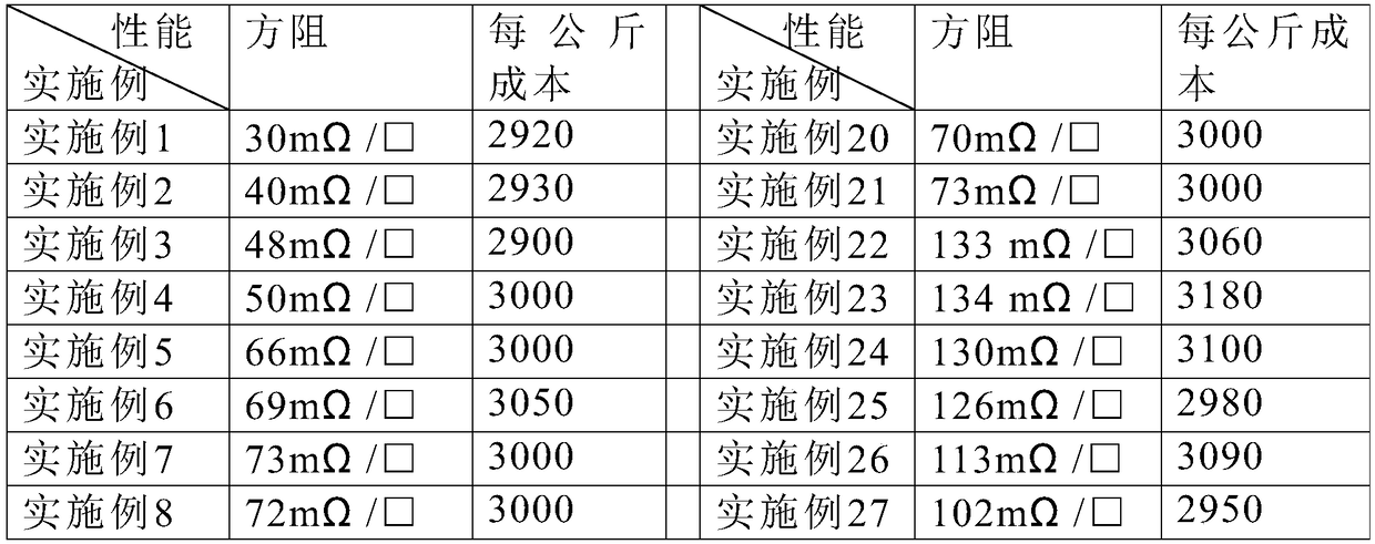
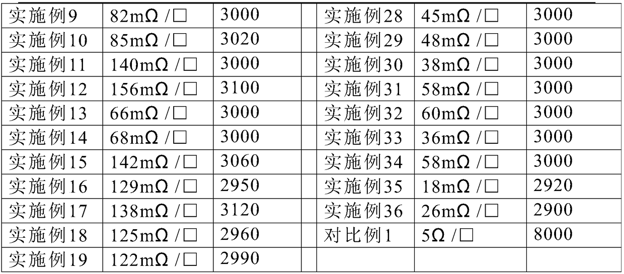
[0026] A thick film circuit resistor paste, comprising 75% solid phase and 25% organic carrier phase accounting for the total mass of the paste, wherein the solid phase includes a conductive functional phase and an inorganic glass bonding phase, and the conductive functional phase is bonded to the inorganic glass The junction phase accounts for 80% and 20% of the total mass of the solid phase respectively, and the conductive functional phase is Zn 2 SnO 4 , Ga 2 o 3 with Bi 2 o 3 complex of Zn 2 SnO 4 , Ga 2 o 3 、 Bi 2 o 3 The mass percentages are 15%, 45%, 40% respectively; the inorganic glass bonding phase is SiO 2 , B 2 o 3 , CaO, ZnO, TiO 2 Composite with NiO, SiO 2 , B 2 o 3 , CaO, ZnO, TiO 2The mass percentages of NiO and NiO are 35%, 9%, 28%, 20%, 6% and 2% respectively; the organic carrier phase is terpineol, tributyl citrate, ethyl cellulose, Span 85, 1, The complexes of 4-butyrolactone and hydrogenated castor oil account for 72%, 14%, 4%, 5%, 4% and...

Embodiment 2

[0028] Compared with Example 1, the only difference is that the thick-film circuit resistor paste of this embodiment includes 70% of the solid phase and 30% of the organic vehicle phase accounting for the total mass of the paste.

Embodiment 3

[0030] Compared with Example 1, the only difference is that the thick-film circuit resistor paste of this embodiment includes 65% of the solid phase and 35% of the organic vehicle phase accounting for the total mass of the paste.


PUM

PropertyMeasurementUnit
particle sizeaaaaaaaaaa

Abstract

The invention relates to resistance paste for a thick film circuit and a preparation method of the resistance paste, in particular to resistance paste for a thin film circuit of a high-power stainlesssteel substrate and a preparation method of the resistance paste and belongs to the technical field of thick film circuits. The resistance paste comprises a solid phase and an organic carrier phase,wherein the solid phase and the organic carrier phase account for 65-85% and 15-35% of total mass of the paste separately; the solid phase comprises a conductive function phase and an inorganic glassbonding phase; and the conductive function phase and the inorganic glass bonding phase account for 55-90% and 10-45% of total mass of the solid phase separately. According to the resistance paste, a cheap semiconductor oxide composite material is adopted as a conductive function phase material of the resistance paste for the thick film circuit of the high-power stainless steel substrate, so that various performance requirements of the resistance paste for the thick film circuit are met, and especially the production cost and the use cost are reduced while the square resistance is greatly reduced. Furthermore, the preparation process provided by the invention is simple in operation, easy to control and beneficial to large-scale industrial production.

Description

technical field [0001] The invention relates to a thick-film circuit resistance slurry and a preparation method thereof, in particular to a high-power stainless steel substrate thick-film resistance slurry and a preparation method thereof, belonging to the technical field of thick-film circuits. Background technique [0002] High-power thick-film resistance heating elements gradually occupy the mainstream position in the high-end water heater market, and the market prospect is very broad. High-power thick-film resistor paste is used to print controllable resistance circuits on substrates, and is the most important electrode material for thick-film resistor heating elements. Stainless steel has the advantages of high mechanical strength, good thermal conductivity, easy processing, and low cost, making it an ideal choice for high-power thick-film circuit substrates. Print and fire the insulating medium layer on the stainless steel substrate, then print and fire the resistor p...

Claims


Application Information

Patent Timeline
Patent Type & Authority Applications(China)
IPC IPC(8): H01B1/20H01B13/00H05B3/14
CPCH01B1/20H01B13/00H05B3/14Y02B30/00
Inventor 袁正勇彭振博倪佳颖
Owner NINGBO POLYTECHNIC
Learn More