Metal-semiconductor composite structure, an SPPs excitation mode and preparation method

A compound structure and semiconductor technology, applied in the field of nanophotonics, can solve the problems of low excitation efficiency, achieve convenient interference, reduce observation difficulty and cost, and achieve high near-field local enhancement effect

Inactive Publication Date: 2018-10-16
HUAZHONG UNIV OF SCI & TECH
View PDF5 Cites 6 Cited by
  • Summary
  • Abstract
  • Description
  • Claims
  • Application Information

AI Technical Summary

Problems solved by technology

[0005] In view of the defects and improvement needs of the prior art, the present invention provides a metal-semiconductor composite structure, SPPs excitation method and preparation method, aiming to solve the problem of low excitation efficiency in the existing SPPs excitation technology

Method used


Image

  • Metal-semiconductor composite structure, an SPPs excitation mode and preparation method
  • Metal-semiconductor composite structure, an SPPs excitation mode and preparation method
  • Metal-semiconductor composite structure, an SPPs excitation mode and preparation method

Examples


Embodiment Construction

[0027] In order to make the object, technical solution and advantages of the present invention clearer, the present invention will be further described in detail below in conjunction with the accompanying drawings and embodiments. It should be understood that the specific embodiments described here are only used to explain the present invention, not to limit the present invention. In addition, the technical features involved in the various embodiments of the present invention described below can be combined with each other as long as they do not constitute a conflict with each other.

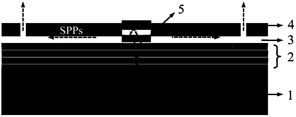
[0028] The metal-semiconductor composite structure provided by the present invention, such as figure 1As shown, it includes: a transparent substrate 1, a multilayer dielectric film 2 on the transparent substrate, a semiconductor nanostructure 5 on the surface of the multilayer dielectric film 2, a transparent dielectric film 3 covering the semiconductor nanostructure, and a transparent dielectri...


PUM


Abstract

The invention discloses a metal-semiconductor composite structure, a SPPs excitation method and a preparation method. The structure sequentially comprises a transparent substrate, a multilayer dielectric film positioned on the transparent substrate, a semiconductor nanostructure positioned on the surface of the multilayer dielectric film, a transparent dielectric thin film for covering the semiconductor nanostructure, and a metal thin film positioned on the transparent dielectric thin film; the semiconductor nanostructure is used for forming defect of a nano scale on the surface of the metal thin film, and generating a fluorescence signal to excite the metal SPPs; the transparent substrate and the multi-layer dielectric film form a double-color-mirror substrate, and the double-color mirrorsubstrate is high in laser transmittance and high in fluorescence reflection; and the excitation method comprises the steps that the laser with relatively short wavelength penetrates through the double-color-mirror substrate and then is vertically incident on the semiconductor nanostructure, so as to excite the semiconductor nanostructure to generate a single-photon fluorescence signal with relatively long wavelength, and then the SPPs of the metal film is excited by the fluorescence signal. According to the invention, the excitation efficiency of the SPPs can be improved, and the detection difficulty and the detection cost of the SPPs can be lowered.

Description

technical field [0001] The invention belongs to the field of nanophotonics, and more specifically relates to a metal-semiconductor composite structure, an SPPs (Surface Plasmon Polaritons, surface plasmon polaritons) excitation method and a preparation method of the composite structure. Background technique [0002] Surface plasmon polaritons (Surface Plasmon Polaritions, SPPs) refer to the collective oscillation of free electrons on the surface of metals and other materials. It is a non-radiative electromagnetic wave propagating along the metal surface, which has good near-field energy localization and sub-wavelength spatial resolution. Metal surface plasmons are widely used in near-field local enhancement and breaking through the optical diffraction limit. Surface plasmons can be excited by electrons or photons. Compared with electronic excitation, optical excitation is more gentle and friendly to the environment, so it is widely used. [0003] When using optical means t...

Claims


Application Information

Patent Timeline
IPC IPC(8): H01S5/10B82Y40/00
CPCB82Y40/00H01S5/10
Inventor 陆培祥胡宏波王凯龙华王兵
Owner HUAZHONG UNIV OF SCI & TECH
Why Eureka
Try Eureka