

Method for preparing copper iodide P-type transparent semi-conductor thin film material at room temperature
A technology of cuprous iodide and thin film materials, which is applied in metal material coating process, ion implantation plating, coating, etc., can solve the problems of low electrical and optical properties, complicated equipment operation, high reaction temperature, etc., and achieve the goal of reaction The effect of high efficiency, simple equipment and short reaction time
- Summary
- Abstract
- Description
- Claims
- Application Information
AI Technical Summary
Problems solved by technology
Method used
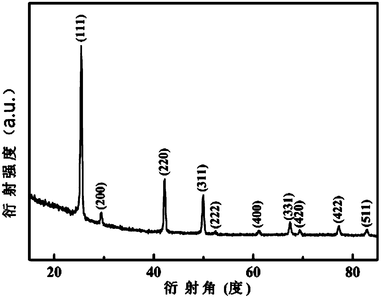
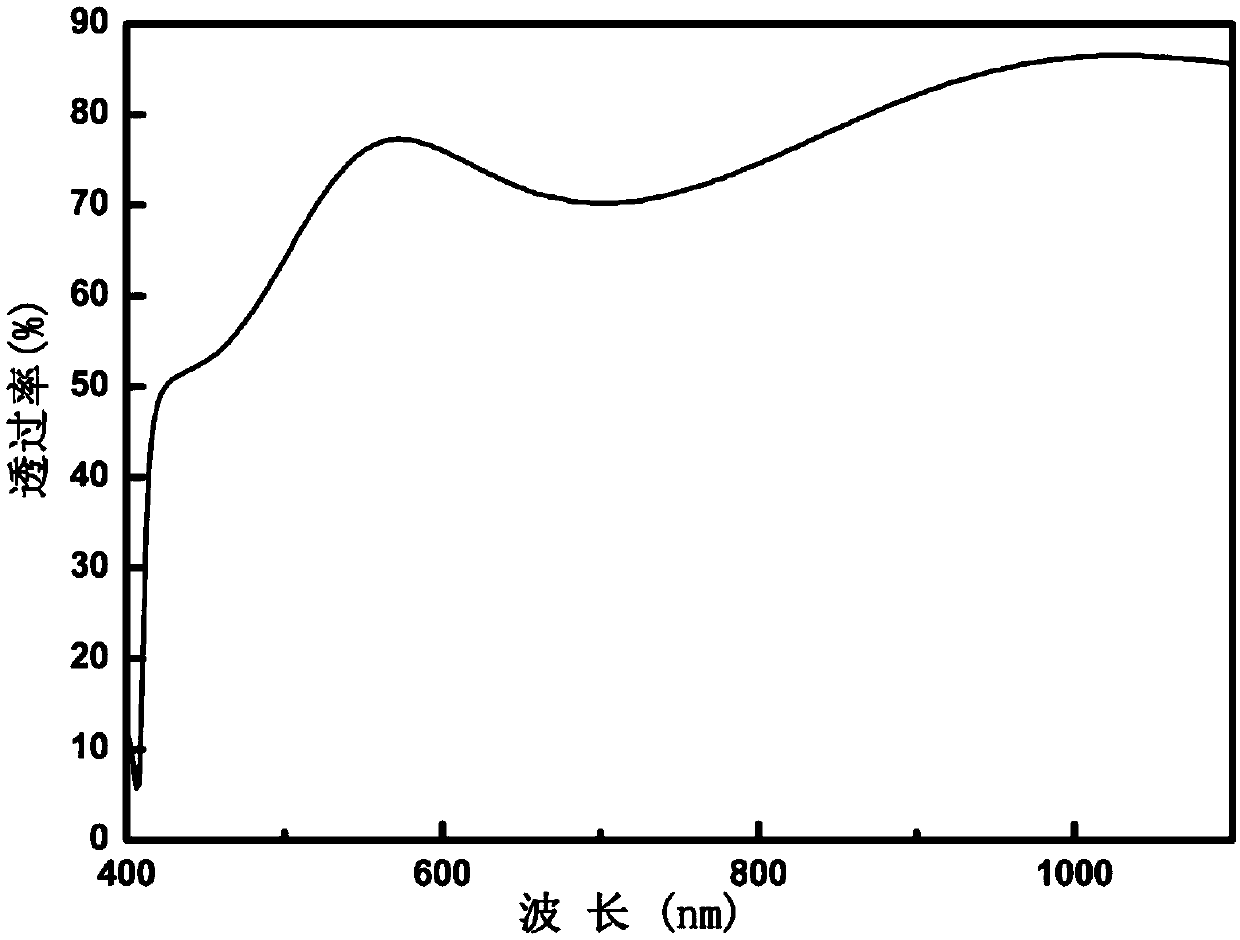
Image

Examples
specific Embodiment approach 1
[0026] Specific embodiment one: the method for preparing cuprous iodide P-type transparent semiconductor film material under a kind of room temperature of present embodiment is to carry out according to the following steps:
[0027] 1. Cleaning of target and substrate:
[0028] Under the condition of ultrasonic power of 200W-400W, the Cu metal target was placed in acetone, alcohol and deionized water for 10min-30min respectively to obtain a clean target; under the condition of ultrasonic power of 50W-150W, the The quartz substrate material with a size of 20mm×20mm×1mm was washed in acetone, alcohol and deionized water for 5min to 15min respectively, and dried to obtain a clean substrate material;
[0029] 2. Preparation of Cu thin film:
[0030] (1) Preparation before coating:
[0031] Install the clean target material to the target position, place the clean substrate material at the center of the sample stage in the high-vacuum magnetron sputtering coating system, and turn ...
specific Embodiment approach 2
[0043]Specific embodiment 2: The difference between this embodiment and specific embodiment 1 is that in step 1, under the condition of ultrasonic power of 200W, the Cu metal target is sequentially placed in acetone, alcohol and deionized water for 15 minutes, respectively, to obtain a clean Under the condition of ultrasonic power of 50W, the quartz substrate material with the size of 20mm×20mm×1mm was washed in acetone, alcohol and deionized water for 5min respectively, and then dried to obtain a clean substrate material. Others are the same as in the first embodiment.
specific Embodiment approach 3
[0044] Embodiment 3: The difference between this embodiment and Embodiment 1 or 2 is that in step 2 (1), the clean target is installed to the target position, and the clean substrate material is placed in high vacuum magnetron sputtering. At the center of the sample stage in the spray coating system, turn on the equipment to vacuum until the vacuum reaches 6×10 -5 Pa. Others are the same as in the first or second embodiment.
PUM
| Property | Measurement | Unit |
|---|---|---|
| thickness | aaaaa | aaaaa |
| particle diameter | aaaaa | aaaaa |
| thickness | aaaaa | aaaaa |
Abstract
Description
Claims
Application Information