
Conducting circuit manufacturing technology for chip

A conductive circuit and manufacturing process technology, applied in the field of conductive circuit manufacturing process of chips, can solve problems such as large pressure difference, uniformity of electroplating metal layer, affecting process uniformity, etc., so as to improve uniformity, effect and efficiency. Effect

Active Publication Date: 2018-10-23
深圳市冠禹半导体有限公司
View PDF4 Cites 0 Cited by
  • Summary
  • Abstract
  • Description
  • Claims
  • Application Information

AI Technical Summary

Problems solved by technology

However, the application of a thin seed layer can lead to problems with the uniformity of plating the metal layer on the seed layer
In the traditional electroplating process, the wafer is in a fixed state, and it is difficult to ensure uniform contact between the wafer and the electroplating solution. At the same time, in order to improve the utilization rate of the wafer, the contact point of the electroplating fixture is usually only connected to the outermost edge of the wafer. The seed layer is in contact, and there is a voltage difference between the seed layer at the center of the wafer and the seed layer at the edge of the wafer, and the thinner the seed layer, the greater the voltage difference
This may cause the plating rate in the central area of ​​the wafer to be much lower than that in the edge area of ​​the wafer, making the coating thickness in the edge area of ​​the wafer larger than that in the central area of ​​the wafer, thereby affecting the uniformity of the process

Method used


Image

  • Conducting circuit manufacturing technology for chip
  • Conducting circuit manufacturing technology for chip
  • Conducting circuit manufacturing technology for chip

Examples


Embodiment Construction

[0029] In order to make the technical means, creative features, goals and effects achieved by the present invention easy to understand, the present invention will be further described below in conjunction with specific embodiments.

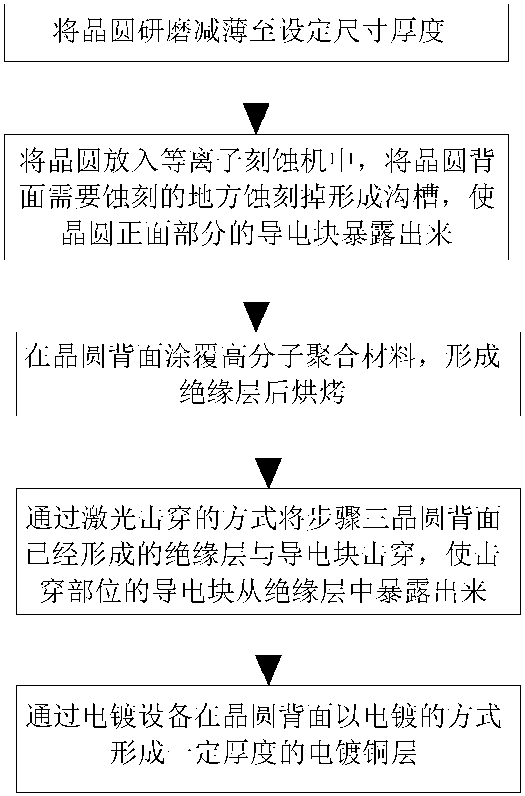
[0030] Such as Figure 1 to Figure 5 As shown, a conductive circuit manufacturing process of a chip according to the present invention, the process comprises the following steps:

[0031] Step 1: Grinding and thinning the wafer to a set size thickness;

[0032] Step 2: After grinding the wafer to a qualified size in step 1, put the wafer into a plasma etching machine, etch away the area to be etched on the back of the wafer to form a groove, exposing the conductive block on the front of the wafer ;

[0033] Step 3: After step 2 is completed, coat the polymer material on the back of the wafer to form an insulating layer and then bake;

[0034] Step 4: Break down the insulating layer and the conductive block that have been formed on the back of t...


PUM


Abstract

The invention belongs to the technical field of semiconductor manufacturing techniques, specifically a conducting circuit manufacturing technology for a chip. Electroplating equipment employed by thetechnology comprises a reaction cavity, magnetic rings, wafers, a holding frame, and a permanent magnet, wherein the electroplating reaction of the wafers is carried out in the reaction cavity. The magnetic rings are horizontally fixed in the reaction cavity, and the magnetic rings are uniformly arranged into multiple layers in the reaction cavity. Each two wafers form one pair, and are arranged in a manner of longitudinal symmetry. The wafers are disposed above the magnetic rings, and the wafers in one group are connected through the holding frame. The edges of the upper and lower wafers of one group are sealed through a sealing plate. The holding frame is located in a closed space of one group of wafers. The permanent magnet is disposed in the holding frame, and the permanent magnet andthe magnetic rings generate acting forces in opposite directions to the wafers, thereby achieving the suspension of the wafers above the magnetic rings. The wafers are suspended in electroplating solution, thereby guaranteeing the uniformity of electroplating. The technology can enable a manufactured conducting circuit to be uniform in thickness and to be good in conductivity.

Description

technical field [0001] The invention belongs to the technical field of semiconductor manufacturing technology, in particular to a chip conductive circuit manufacturing technology. Background technique [0002] Wafer (Wafer) refers to the silicon wafer used in the production of silicon semiconductor integrated circuits. Because of its circular shape, it is called a wafer. Electroplate a layer of conductive metal on the wafer, and process the conductive metal layer to make conductive lines. Electroplating is one of the key processes for making these metal layers. Wafer electroplating is to place the wafer in the electroplating solution, apply the voltage negative electrode to the thin metal layer (seed layer) prefabricated on the wafer, and apply the voltage positive electrode to the On the soluble or insoluble anode, the metal ions in the plating solution are deposited on the surface of the wafer through the action of an electric field. [0003] With the development of semi...

Claims


Application Information

Patent Timeline
IPC IPC(8): H01L21/60C25D7/12C25D17/00
CPCC25D7/12C25D17/001H01L24/03H01L2224/02317
Inventor 李涵孙勇
Owner 深圳市冠禹半导体有限公司
Features
  • Generate Ideas
  • Intellectual Property
  • Life Sciences
  • Materials
  • Tech Scout
  • Unparalleled Data Quality
  • Higher Quality Content
  • 60% Fewer Hallucinations
Learn More