Organic semiconductor composition, organic thin film comprising same, and use thereof
一种有机薄膜、组合物的技术,应用在半导体器件、半导体/固态器件制造、有机化学等方向,能够解决印刷适应性不明确等问题
- Summary
- Abstract
- Description
- Claims
- Application Information
AI Technical Summary
Problems solved by technology
Method used
Image


Examples
Embodiment 1
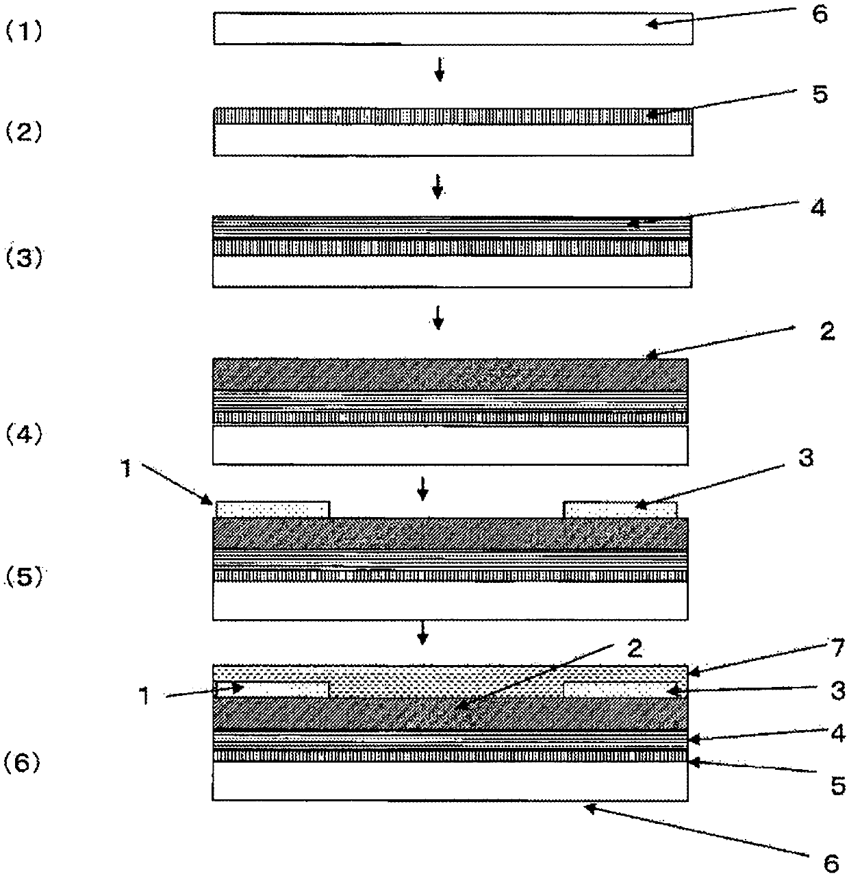
[0164] Example 1 (composition of the present invention, organic thin film forming material comprising the composition, and organic thin film obtained using the forming material)
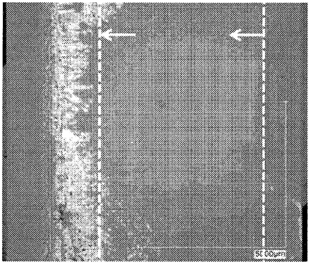
[0165] Compounds No.1 and No.3 of the specific example were dissolved in chlorobenzene at a mass ratio of No.1:No.3=9:1 so that the total concentration of the compounds became 0.1%. This solution was dropped onto a silicon substrate having a silicon oxide film of 100 nm, blade-coated at a rate of 2.5 μm / sec using a glass doctor blade, and then dried at 70° C. The film thickness of the obtained organic thin film is about 9nm, such as image 3 (In the figure, the arrow indicates the scanning direction of the glass scraper, and the dotted line indicates the area where the film is effectively formed in the method described in this example.) As shown, a homogeneous film with no cracks in a wide range was obtained. film.
Embodiment 2
[0166] Example 2 (composition of the present invention, organic thin film forming material comprising the composition, and organic thin film obtained using the forming material)
[0167] In addition to dissolving the specific example compounds No.1 and No.3 in chlorobenzene at a mass ratio of No.1:No.3=5:5, the total concentration of the compounds becomes 0.1%, and An organic thin film was produced in the same manner as in Example 1. The polarizing microscope image of the obtained organic film is as Figure 4 As shown, a homogeneous film without cracks in a wide range was obtained.
Embodiment 3
[0168] Example 3 (Composition of the present invention, organic thin film forming material comprising the composition, and organic thin film obtained using the forming material)
[0169] In addition to dissolving the specific example compounds No.1 and No.3 in chlorobenzene at a mass ratio of No.1:No.3=3:7 so that the total concentration of the compounds becomes 0.1%, and An organic thin film was produced in the same manner as in Example 1. The film thickness of the obtained organic thin film is 9 to 18nm, and polarizing microscope image is as Figure 5 As shown, a homogeneous film without cracks in a wide range was obtained.
PUM
| Property | Measurement | Unit |
|---|---|---|
| coating thickness | aaaaa | aaaaa |
| boiling point | aaaaa | aaaaa |
| solubility coefficient | aaaaa | aaaaa |
Abstract
Description
Claims
Application Information
PatSnap Eureka turns technology decisions into work you can execute. Powered by our Innovation Knowledge Graph, it runs expert workflows across engineering, life sciences, materials and intellectual property. Get your review-ready output in minutes.


