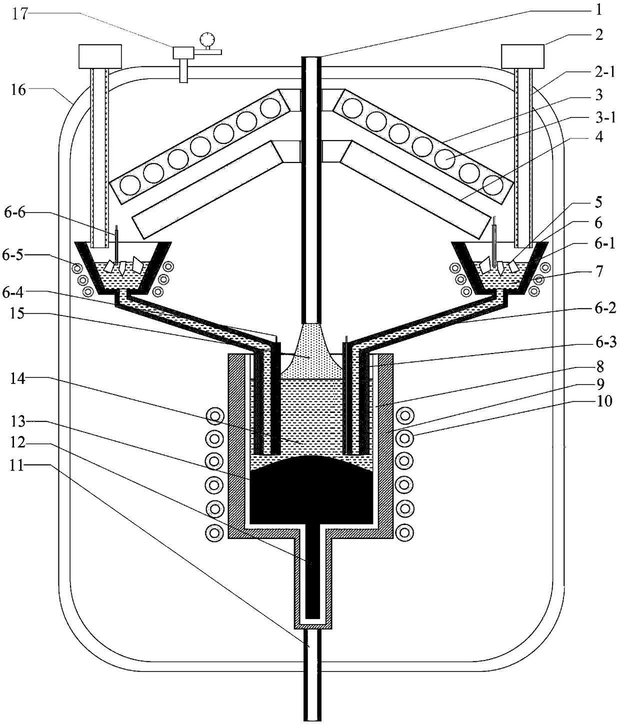
Gallium nitride single crystal growth device

A technology of gallium nitride single crystal and growth device, applied in single crystal growth, single crystal growth, crystal growth and other directions, can solve the problems of expensive preparation, growing GaN single crystal, difficult to prepare GaN single crystal, etc.

CN108707961AInactive Publication Date: 2018-10-26孟静
0 Cites 2 Cited by

Patent Information

Authority / Receiving Office
CN · China
Patent Type
Applications(China)
Current Assignee / Owner
Publication Date
2018-10-26
Estimated Expiration
Not applicable · inactive patent

Smart Images

  • Figure 1
    Figure 1
Patent Text Reader

Abstract

The invention discloses a gallium nitride single crystal growth device, and relates to the technical field of semiconductor material preparation devices. The device mainly uses a nitrogen plasma evaporation reflux method to form a supersaturated melt on a crystal growth interface to prepare a gallium nitride crystal. Nitrogen plasma is used for volatilizing a fluxing gallium-sodium-nitrogen melt,gallium and sodium elements are volatilized at a high temperature and cooled on a condenser to form a gallium-sodium melt. The gallium-sodium melt is refluxed into a reflux system, sodium nitride is continuously put into the reflux system, the thermal decomposition of the sodium nitride makes the melt keep in a nitrogen saturated state, and the saturated melt is refluxed onto a high-temperature solid-liquid interface to form a supersaturated melt for crystal growth.
Need to check novelty before this filing date? Find Prior Art

Description

technical field

[0001] The invention relates to the technical field of semiconductor material preparation devices, in particular to a gallium nitride single crystal growth device. Background technique

[0002] Gallium nitride (GaN) is a wide bandgap semiconductor material with a bandgap as high as 3.4eV. It is mainly used in the preparation of microwave power transistors and blue light-emitting devices. It can produce higher power, higher efficiency, Larger broadband microwave devices can produce high conversion efficiency, high operating frequency, high temperature power electronic devices. It is widely used in the fields of communication, satellite, aerospace and aviation, especially with the coming of 5G, GaN will usher in explosive growth.

[0003] Because the pressure of directly preparing GaN by the melt method is very high, which needs to reach 93Kbar (2427°C), it is difficult to grow GaN single crystal directly by the melt method. Metal organic compound chemical va...

Examples

Embodiment Construction

[0012] The technical solutions in the embodiments of the present invention are clearly and completely described below in conjunction with the accompanying drawings in the embodiments of the present invention. Obviously, the described embodiments are only part of the embodiments of the present invention, not all of them. Based on the embodiments of the present invention, all other embodiments obtained by persons of ordinary skill in the art without making creative efforts belong to the protection scope of the present invention.

[0013] In the following description, a lot of specific details are set forth in order to fully understand the present invention, but the present invention can also be implemented in other ways different from those described here, and those skilled in the art can do it without departing from the meaning of the present invention. By analogy, the present invention is therefore not limited to the specific examples disclosed below.

[0014] Such as figure ...