A semiconductor silicon wafer rotary lithography machine

A silicon wafer and semiconductor technology, which is applied in the field of semiconductor silicon wafer rotary lithography machines, can solve the problem that the shock absorption effect of a shock absorber cannot achieve the expected effect, etc., so as to increase the shock absorption pressure, save the usage amount, and improve the usage. effect of life

Active Publication Date: 2020-08-04
SHAOXING NIKER AUTOMOBILE ACCESSARY
View PDF1 Cites 0 Cited by
  • Summary
  • Abstract
  • Description
  • Claims
  • Application Information

AI Technical Summary

Problems solved by technology

However, the elimination of the vibration of the silicon wafer table in this scheme does not give an exact solution; and the damping effect of the shock absorber between the main frame and the base frame cannot reach the expected effect

Method used


Image

  • A semiconductor silicon wafer rotary lithography machine
  • A semiconductor silicon wafer rotary lithography machine
  • A semiconductor silicon wafer rotary lithography machine

Examples


Embodiment approach

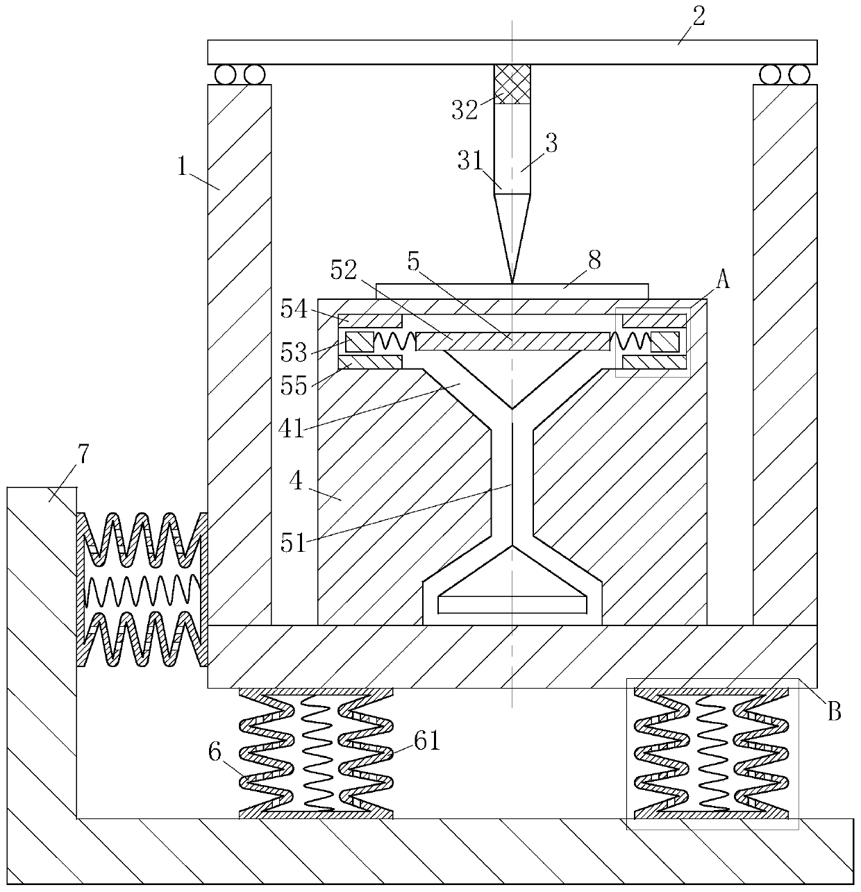
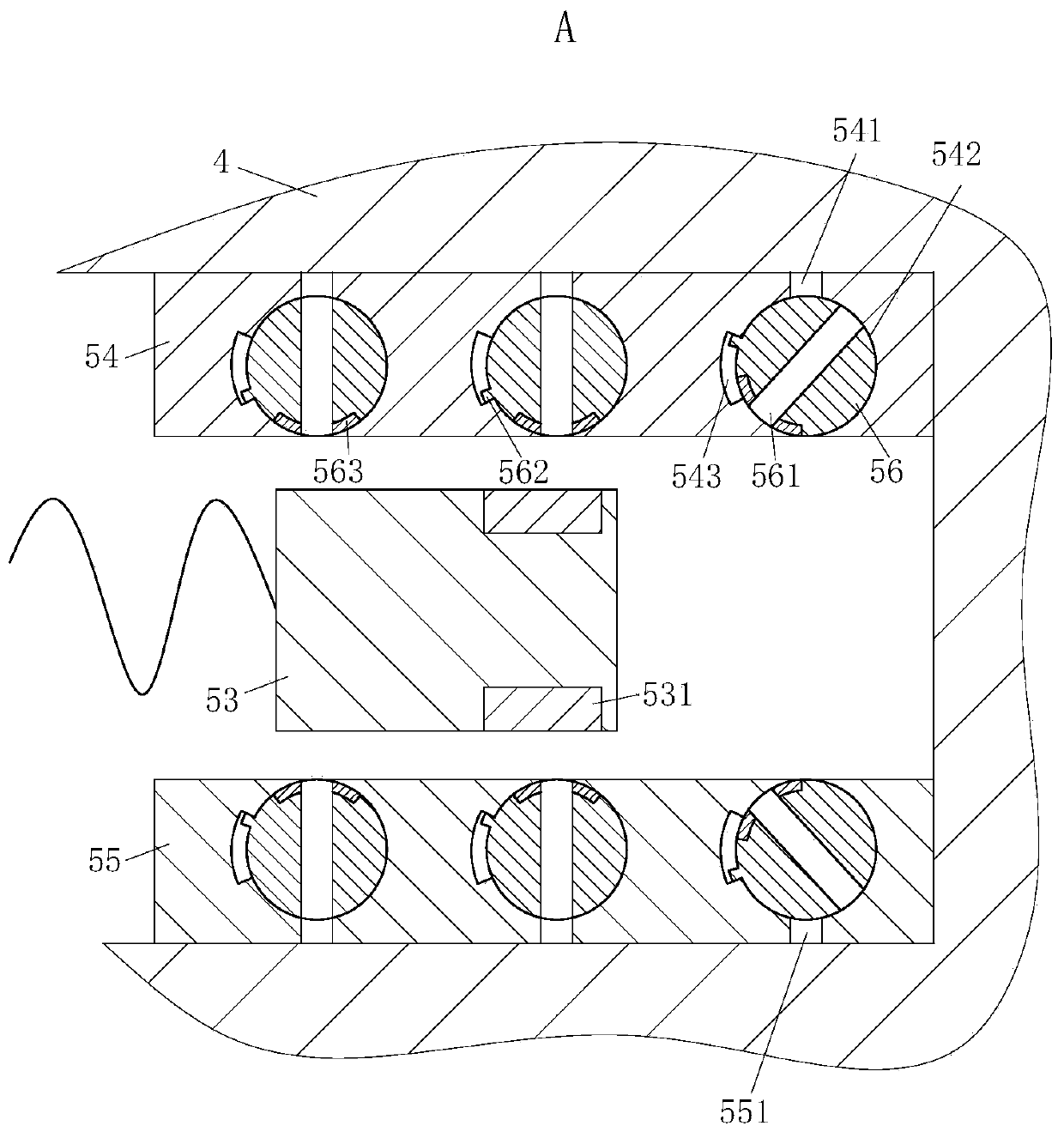
[0025] As an embodiment of the present invention, a No. 1 spherical cavity 542 is set in the No. 1 blowing hole 541 and No. 2 blowing hole 551; a No. 1 circular arc is set on the side of the No. 1 spherical cavity 542 close to the central turntable 52 Shape chute 543; Rotation block 56 is installed in the No. 1 spherical cavity 542; No. 4 blowing holes 561 are set inside the rotation block 56, and sliding boss 562 is set on the side of rotation block 56 near the center turntable 52; The sliding boss 562 slides in the No. 1 arc-shaped chute 543; the No. 4 air blowing hole 561 is embedded in a circular spherical magnet 563 near the outlet of one end of the balance weight 53; the upper and lower surfaces of the balance weight 53 are embedded with magnets 531 . The higher the motor speed, the greater the centrifugal force on the balance weight 53, the farther the balance weight 53 from the center of rotation, the farther the distance, the more openings on the upper and lower air f...


PUM


Abstract

The invention belongs to the technical field of semiconductor manufacture, and specifically relates to a semiconductor silicon wafer rotary mask aligner. The semiconductor silicon wafer rotary mask aligner comprises a main frame, a mobile support, an exposure device, a rotary table, a dynamic balance device, a damping device, and a base frame, wherein the main frame is internally provided with therotary table, the mobile support is installed above the main frame in a sliding manner, the middle lower part of the mobile support is fixedly connected with the exposure device, the rotary table isarranged below the exposure device, the rotary table is internally provided with the dynamic balance device, the dynamic balance device is used for reducing vibration generated by the rotary table inrotation, the damping device is arranged between the main frame and the base frame, and the damping device is used for reducing vibration generated by the main frame. In the semiconductor silicon wafer rotary mask aligner, the dynamic balance device is arranged in a rotary cavity, so that vibration generated by the rotary table in rotation is reduced; and the damping device is arranged between themain frame and the base frame, so that vibration generated by the main frame is reduced.

Description

technical field [0001] The invention belongs to the technical field of semiconductor manufacturing, in particular to a semiconductor silicon wafer rotary photolithography machine. Background technique [0002] Wafer refers to the silicon chip used in the production of silicon semiconductor integrated circuits. Wafer is the carrier used in the production of integrated circuits. In general, wafers refer to single crystal silicon wafers. Wafers are the most commonly used semiconductor materials. In the production process of integrated circuit chips, the exposure and transfer of chip design patterns on the photoresist on the surface of silicon wafers is one of the most important processes. The equipment used in this process is called a photolithography machine. Lithography machine is the most critical equipment in the process of integrated circuit processing. Foreign countries have proposed the concept of next-generation lithography many years ago, and have conducted a lot of r...

Claims


Application Information

Patent Timeline
Patent Type & Authority Patents(China)
IPC IPC(8): G03F7/20
CPCG03F7/70716G03F7/709G03F7/70916
Inventor 侯玉闯薛鹏
Owner SHAOXING NIKER AUTOMOBILE ACCESSARY
Why Eureka
Try Eureka