Common-caliber frequency reconfigurable on-chip slit array antenna and use method

A technology for slot array antennas and array antennas, which is applied in antennas, antenna arrays, specific array feeding systems, etc., and can solve problems such as difficult suppression of mutual coupling, limited number of lumped elements, and difficulties in assembly and debugging of reconfigurable antennas , to achieve the effect of increasing degrees of freedom and reducing complexity

Active Publication Date: 2018-10-26
NANJING UNIV OF AERONAUTICS & ASTRONAUTICS
View PDF8 Cites 14 Cited by
  • Summary
  • Abstract
  • Description
  • Claims
  • Application Information

AI Technical Summary

Problems solved by technology

[0003] Under the premise of a common aperture, the array antenna of the traditional radio system covers a wider frequency band by using a multi-layer microstrip antenna to place array antennas of different frequencies on different levels, and then adding a feeding device to it. The structure of the antenna It is too complicated, and the mutual coupling of channels between different frequencies is difficult to suppress, and the antenna structure needs to be reconfigurable to meet the needs of use at different frequencies
[0004] The traditional method to achieve an...

Method used


Image

  • Common-caliber frequency reconfigurable on-chip slit array antenna and use method
  • Common-caliber frequency reconfigurable on-chip slit array antenna and use method
  • Common-caliber frequency reconfigurable on-chip slit array antenna and use method

Examples


Embodiment Construction

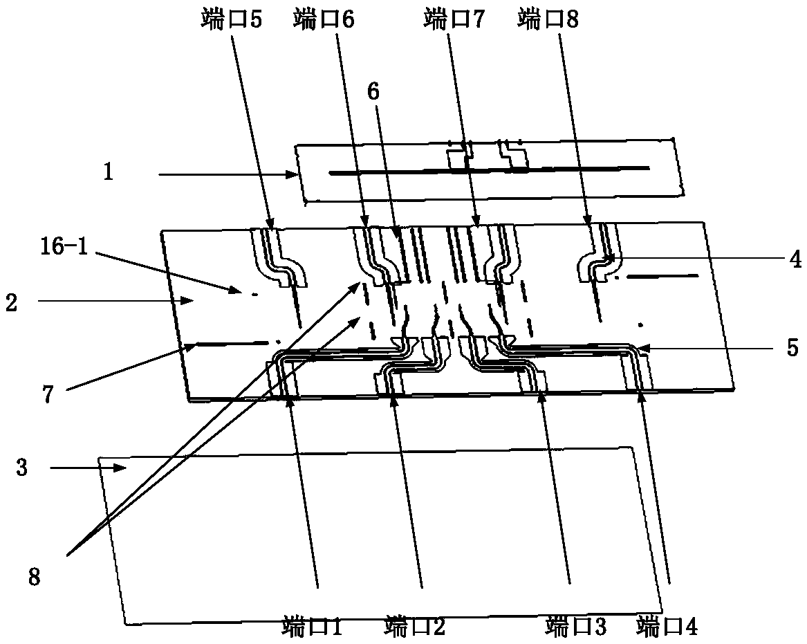
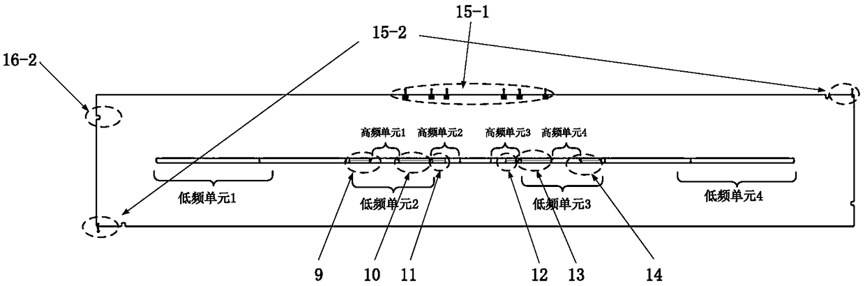
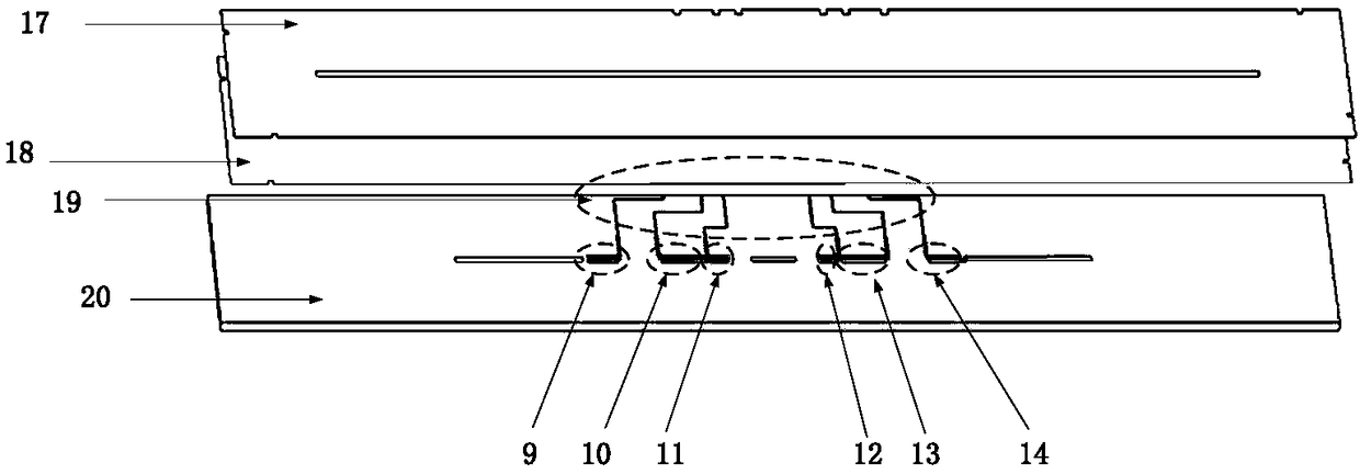
[0027] Such as Figure 1 to Figure 6 As shown, a frequency reconfigurable on-chip slot array antenna is characterized in that it includes a silicon-based reconfigurable slot radiator layer (1), a PCB feeder layer (2), and a metal reflection cavity ( 3); the silicon-based reconfigurable radiator layer includes a metal layer (17) covered on the upper surface of the intrinsic silicon layer, an S-PIN unit (9-14) loaded at a specific position in the metal gap, and an S-PIN unit (9-14) for the S- PIN units apply DC bias on-chip wiring (19) and gold wire jumpers (15-1), (15-2) and other structures, and the S-PIN loaded in the gap adopts a "back-to-back" PIN tube design, that is N-P-N settings. Such as Figure 7 , the on-chip routing of the DC feeder adopts a "serpentine bending" structure (19), one end of which is connected to the P+ region (22) of the S-PIN unit, and the other end is drawn to the edge of the silicon-based reconfigurable radiator layer through the pad (21) Connect...


PUM


Abstract

The invention provides a common-caliber frequency reconfigurable on-chip slit array antenna and a use method. The antenna comprises a silicon-based reconfigurable radiator layer, a PCB feeder line layer, a jumper line connection structure of a PCB and a silicon-base radiator, and a metal reflection cavity. The silicon-based reconfigurable radiator layer comprises a metal layer, multiple surface P-I-N diode (S-PIN) units, an insulation isolation layer, an S-PIN direct current bias layer and an intrinsic silicon medium layer, wherein slits are etched in the metal layers and the surface P-I-N diode (S-PIN) units are connected into the slits of the metal layer in a crossing manner. The PCB feeder line layer comprises a direct current lead connected with the silicon-based reconfigurable radiator layer, a microwave feeding device and a structure aligned to the silicon-based reconfigurable radiator layer. The reflection face layer is achieved by use of a metal box body. According to the invention, by controlling on and off of the S-PIN units connected into the metal slits of the silicon-based reconfigurable radiator layer in a crossing manner, working frequency and unit intervals of the array antenna are controlled, and frequency reconfiguration of the slit array antenna is finally achieved. Meanwhile, by use of the novel silicon-based S-PIN bias technology, radiation characteristicsof reconfigurable antenna are improved.

Description

technical field [0001] The invention relates to a frequency reconfigurable on-chip slot array antenna, in particular to a frequency reconfigurable on-chip slot array antenna using silicon-based semiconductor S-PIN technology, and belongs to the technical field of reconfigurable on-chip array antennas. Background technique [0002] As one of the core components that affect the performance of radar systems and communication systems, the antenna system has a decisive impact on system functions. On this basis, people hope to use as few antennas as possible to meet the requirements of all wireless systems. However, these The working frequency of the radio system is usually distributed in a very wide frequency band, and the reconfigurability of a wide frequency span can make the front end of the radio system more compact and the whole system more miniaturized. In addition, radio systems often employ array antennas as radio transmitters. Array antennas in a wide frequency range ha...

Claims


Application Information

Patent Timeline
IPC IPC(8): H01Q1/38H01Q1/50H01Q5/321H01Q19/10H01Q21/00
CPCH01Q1/38H01Q1/50H01Q5/321H01Q19/10H01Q21/0006
Inventor 周永刚刘少斌闻乐天陈鑫唐丹
Owner NANJING UNIV OF AERONAUTICS & ASTRONAUTICS
Why Eureka
Try Eureka