[0049] In order to clearly illustrate the technical features of the present solution, the present invention will be described in detail below through specific implementations and in conjunction with the accompanying drawings. The following disclosure provides many different embodiments or examples for implementing different structures of the present invention. In order to simplify the disclosure of the present invention, the components and settings of specific examples are described below. In addition, the present invention may repeat reference numbers and/or letters in different examples. This repetition is for the purpose of simplification and clarity, and does not in itself indicate the relationship between the various embodiments and/or settings discussed. It should be noted that the components illustrated in the drawings are not necessarily drawn to scale. The present invention omits descriptions of well-known components and processing techniques and processes to avoid unnecessarily limiting the present invention.
[0050] The following describes in detail a method and system for optimizing a high-speed signal of a reference clock line provided by embodiments of the present invention with reference to the accompanying drawings.
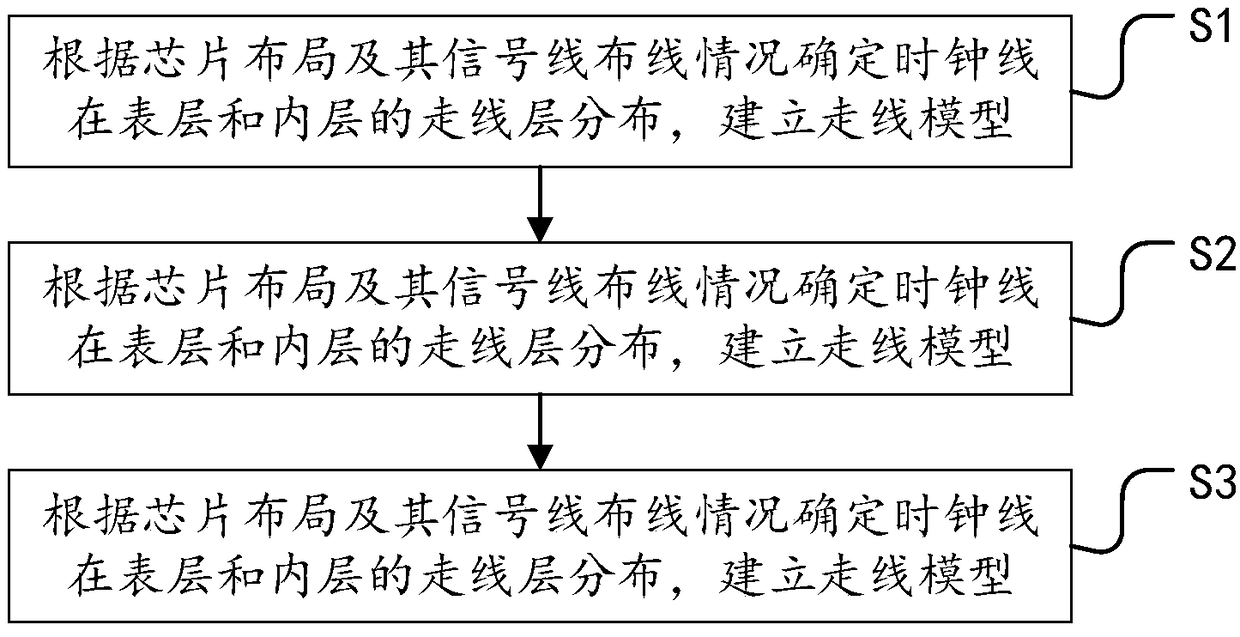
[0051] Such as figure 1 As shown, the embodiment of the present invention discloses a method for optimizing a high-speed signal of a reference clock line, which includes the following steps:
[0052] S1. Determine the wiring layer distribution of the clock line on the surface and the inner layer according to the chip layout and its signal line wiring, and establish a wiring model;
[0053] S2. Obtain the stacking information of the simulated waveform based on the wiring model, and evaluate the propagation speed of the signal on the surface and the inner layer;
[0054] S3. Set the trace length of the surface layer and the inner layer according to the signal propagation speed combined with equal length requirements and delay requirements.
[0055] Since the propagation speed of the clock line is different when routing on different PCB layers, it is necessary to measure the propagation speed of the clock line on different routing layers.
[0056] Determine the routing layer distribution of the clock line according to the chip layout and its signal line wiring. Take a specific link as an example. The reference clock link is distributed on the surface and the inner layer. The reference clock from the clock source to the CPU is distributed on the surface. , About 15 inches; the reference clock from the clock source to the device is distributed in the inner layer, about 18 inches.
[0057] After the wiring model is established, the propagation speed of the clock signal in different wiring layers is evaluated according to the lamination information of the surface and inner wiring models, as follows:
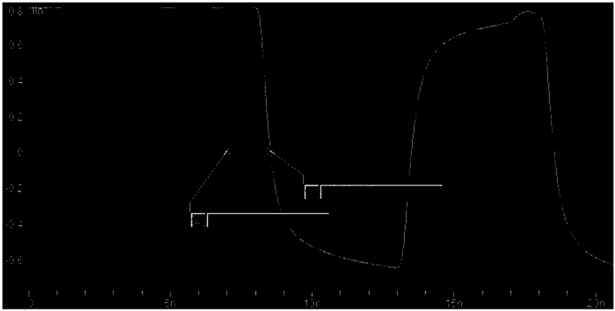
[0058] First, evaluate the propagation speed of the clock signal on the surface. When the trace length of the signal line in the surface layer is 18inch and 28inch, the signal waveform is simulated by the simulation software, and the waveform at the receiving end is as follows figure 2 As shown, the time difference between the two traces when the signal reaches the receiving end is about 1.55ns. It can be estimated that the propagation speed of the clock signal on the surface is about 6.45inch/ns (for the convenience of subsequent calculations, the surface propagation speed is converted to 155ps/inch) .
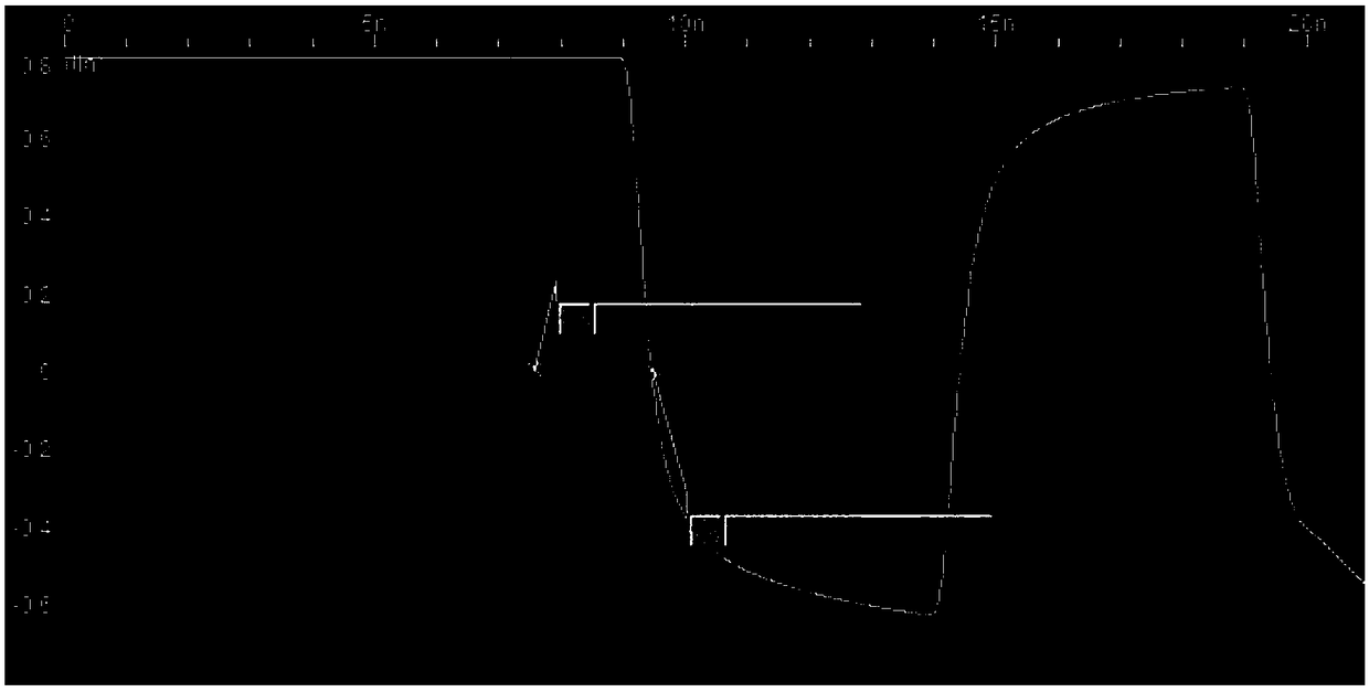
[0059] Second, evaluate the propagation speed of the clock signal in the inner layer. When the signal line in the inner layer is 18inch and 28inch, the signal waveform is simulated by the simulation software, and the waveform at the receiving end is as follows image 3 As shown, the time difference between the two traces when the signal reaches the receiving end is about 1.88ns. It can be estimated that the propagation speed of the clock signal on the surface is about 5.32inch/ns (for the convenience of subsequent calculations, the inner layer propagation speed is converted to 188ps/inch ).
[0060] According to the design requirements of the clock line equal length, the two must meet the 5inch equal length design, that is, the difference between the surface and inner clock line lengths is no more than 5 inches. Based on the surface wiring evaluation, the maximum allowable signal transmission delay is:
[0061]
[0062] ΔT is the transmission delay, ΔS is the maximum length difference, V surface layer Is the surface transmission speed.
[0063] When the two need to meet the 5inch maximum length difference, the maximum allowable signal transmission delay is 755ps.
[0064] Taking the example of the reference clock link in the embodiment of the present invention, the surface wiring is 15 inches and the inner wiring is 18 inches. Although it meets the design requirements of equal length, the delay is about 1060 ps, which cannot meet the design requirements of delay. Delayed waveform such as Figure 4 Shown.
[0065] Therefore, it is necessary to set the length of each wiring layer in combination with equal length requirements and delay requirements.
[0066] The length of each wiring layer is preferably routed around the long surface layer, specifically:
[0067]
[0068] S surface layer =V surface layer *T
[0069] T is the wiring time, S surface layer Is the length of the surface trace.
[0070] When the inner layer propagation speed is 5.32inch/ns, the inner layer trace length is 18inch, and the corresponding surface layer trace length is 21.8±4.9inch, that is, 16.9inch to 26.7inch.
[0071] When the long surface layer is routed to 18 inches, the simulation waveform is as Figure 5 As shown, the delay of the two is 600ps, which meets the delay requirement.
[0072] The setting of the length of each wiring layer can also shorten the inner wiring, specifically:
[0073]
[0074] S Inner layer =V Inner layer *T
[0075] T is the wiring time, S Inner layer Is the length of the inner wiring.
[0076] When the surface propagation speed is 6.45inch/ns, the surface trace length is 15inch, and the corresponding surface trace length is 12.4±4inch, that is, 8.4inch to 16.4inch.
[0077] In the embodiment of the present invention, the wiring layer distribution of the clock line is determined, and the signal propagation speed of each wiring layer is calculated according to the lamination information of the simulation waveform, and finally the length of each wiring layer is set according to the equal length requirement and the delay requirement, thereby Realize the optimal design of the clock signal line, avoid blindly pursuing the physical isometric design of the signal line and neglect the more critical delay requirements. On the basis of not only meeting the physical isometric length, but also meeting the delay requirements, making the design more It is reasonable, reduces the design risk of the link, improves the success rate of the system design, and enhances the signal quality.
[0078] Such as Image 6 As shown, the embodiment of the present invention also discloses a high-speed signal optimization system of a reference clock line, including:
[0079] The wiring layer distribution determination module is used to determine the wiring layer distribution of the clock line on the surface and the inner layer according to the chip layout and its signal line wiring conditions, and establish a wiring model;
[0080] The propagation speed determination module is used to obtain the stacking information of the simulated waveform based on the routing model, and to evaluate the propagation speed of the signal on the surface and the inner layer;
[0081] The wiring layer length determination module is used to set the wiring length of the surface layer and the inner layer according to the signal propagation speed combined with equal length requirements and delay requirements.
[0082] The requirement of equal length is specifically that the difference between the trace length of the surface layer and the inner layer does not exceed 5 inches.
[0083] The delay requirements are as follows:
[0084] The maximum allowable signal transmission delay is:
[0085]
[0086] ΔT is the transmission delay, ΔS is the maximum length difference, V surface layer Is the surface transmission speed.
[0087] The wiring layer length determining module includes:
[0088] The long surface wiring unit is used to set the surface wiring length. The calculation formula for the surface wiring length is:
[0089]
[0090] S Inner layer =V Inner layer *T
[0091] T is the wiring time, S Inner layer Is the inner wiring length;
[0092] The inner wiring unit is shortened to set the inner wiring length. The calculation formula for the inner wiring length is:
[0093]
[0094] S Inner layer =V Inner layer *T
[0095] T is the wiring time, S Inner layer Is the length of the inner wiring.
[0096] The above are only the preferred embodiments of the present invention and are not intended to limit the present invention. Any modification, equivalent replacement and improvement made within the spirit and principle of the present invention shall be included in the protection of the present invention. Within range.