Mechanical chuck and semiconductor processing equipment

A technology for mechanical chucks and workpieces, which is applied in semiconductor/solid-state device manufacturing, metal material coating technology, ion implantation plating, etc., can solve the problem of reducing the use efficiency and processing efficiency of PVD equipment, increasing the weight of snap ring 3, It takes a long time and other problems to achieve the effect of shortening the time of machine switching, reducing the workload and reducing the workload

Active Publication Date: 2018-11-13
BEIJING NAURA MICROELECTRONICS EQUIP CO LTD
View PDF7 Cites 6 Cited by
  • Summary
  • Abstract
  • Description
  • Claims
  • Application Information

AI Technical Summary

Problems solved by technology

[0005] In practical applications, in order to improve the efficiency of PVD equipment, the same PVD equipment is often used to process wafers of different sizes (such as 12-inch wafers and 8-inch wafers). 3 and the size of the sputtering ring 5 are different, that is, the machines corresponding to processing wafers of different sizes are not compatible
Therefore, when processing wafers of different sizes, it is necessary to replace the matching machine, that is, the inner shield 2, the snap ring 3 and the sputtering ring 5 need to be replaced. Use efficiency and processing efficiency
[0006] In addition, when using the machine for processing 12-inch wafers to process 8-inch wafers, the outer diameter of the snap ring 3 corresponding to the 8-inch wafers needs to be enlarged to match the size of the inner shield 2 corresponding to the 12-inch wafers, which will inevitably increase Due to the weight of the snap ring 3, it is easy to crush the wafer due to the heavy weight of the snap ring 3

Method used


Image

  • Mechanical chuck and semiconductor processing equipment
  • Mechanical chuck and semiconductor processing equipment
  • Mechanical chuck and semiconductor processing equipment

Examples


Embodiment Construction

[0051] In order to enable those skilled in the art to better understand the technical solution of the present invention, the mechanical chuck and semiconductor processing equipment provided by the present invention will be described in detail below with reference to the accompanying drawings.

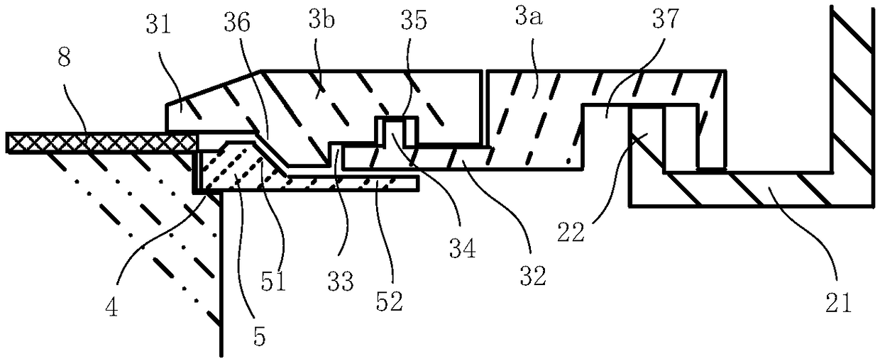
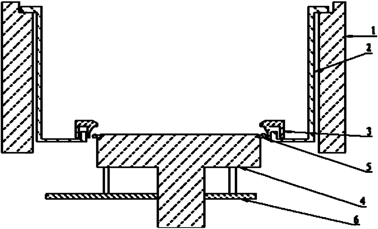
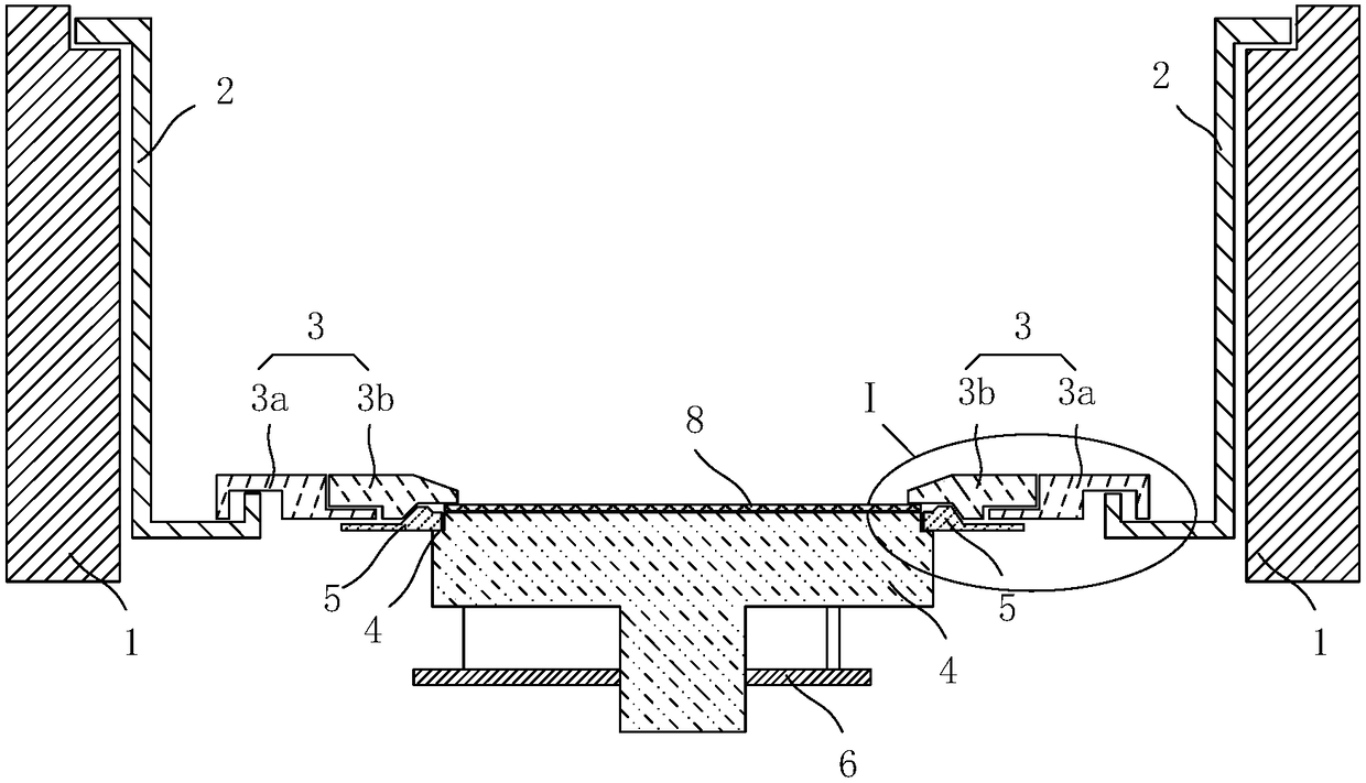
[0052] figure 2 A partial cross-sectional view of the semiconductor processing equipment provided by the embodiment of the present invention, image 3 for figure 2 Enlarged view of the middle I region. Please refer to figure 2 with image 3 , the semiconductor processing equipment includes a reaction chamber 1, an inner shield 2 is fixed on the inner side wall of the reaction chamber 1, and is used to prevent the target metal from being sputtered to the bottom of the reaction chamber 1 during the sputtering process. The inner shield 2 is a barrel-shaped structural member arranged around the inner wall of the reaction chamber 1, the bottom end of the inner shield 2 is provided with ...


PUM


Abstract

The invention provides a mechanical chuck and semiconductor processing equipment. The mechanical chuck includes a pedestal, a sputtering ring and a snap ring. The top surface of the pedestal is used for bearing a to-be-processed member. The sputtering ring sleeves the outside of the top part of the pedestal. The snap ring includes a first snap ring component and a second snap ring component whichare arranged in an inside and outside nesting manner, wherein the first snap ring component is arranged on the outer side and the second snap ring component is arranged on the inner side. The first snap ring component and the second snap ring component are superimposed on the upper surface of the sputtering ring. The second snap ring component laminates the edge area of the to-be-processed memberso as to fix the to-be-processed member to the top surface of the pedestal. The mechanical chuck is high in switching efficiency and can prevent the to-be-processed member from being crushed.

Description

technical field [0001] The invention belongs to the field of semiconductor manufacturing, and in particular relates to a mechanical chuck and a semiconductor processing device. Background technique [0002] During the manufacturing process of integrated circuits, physical vapor deposition (Physical Vapor Deposition, hereinafter referred to as PVD) technology is usually used to deposit metal materials on the surface of the wafer. With the maturity and wide application of Through Silicon Via (TSV) technology, PVD technology is applied to deposit a barrier layer and a copper seed layer inside the Silicon Via. [0003] In PVD equipment, electrostatic chucks and mechanical chucks are two common methods used to hold wafers. The electrostatic chuck uses electrostatic attraction to fix the wafer. However, when the deposition process of through-silicon vias is implemented, due to the large thickness and stress of the film deposited in the through-silicon vias, the electrostatic chuc...

Claims


Application Information

Patent Timeline
Patent Type & Authority Applications(China)
IPC IPC(8): C23C14/50H01L21/687
CPCC23C14/50H01L21/68721
Inventor 王涛
Owner BEIJING NAURA MICROELECTRONICS EQUIP CO LTD
Why Eureka
Try Eureka