Packing structure for RF microwave power amplifier

A packaging structure and RF power amplifier technology, applied in the direction of electric solid-state devices, semiconductor devices, semiconductor/solid-state device components, etc., can solve the problems of thin-film circuit customization, low capacitance precision, and long R&D cycle, etc., to improve heat dissipation effect, Reduce the R&D cycle and improve performance

Pending Publication Date: 2018-11-13
苏州本然微电子有限公司
View PDF0 Cites 2 Cited by
  • Summary
  • Abstract
  • Description
  • Claims
  • Application Information

AI Technical Summary

Problems solved by technology

Such a design mainly has the following disadvantages: (1) The thin film circuit needs to be customized, the development cycle is long, and the cost is high
Difficulty in debugging is also the main disadvantage; (2) Customized RF power amplifier chip capacitors have low capacitance accuracy, high cost, and are not easy to debug
(3) If the IPD process is adopted, the R&D cycle will be longer and the cost will be higher

Method used


Image

  • Packing structure for RF microwave power amplifier
  • Packing structure for RF microwave power amplifier
  • Packing structure for RF microwave power amplifier

Examples


Embodiment 1

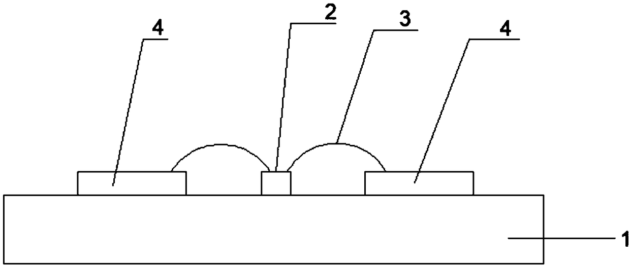
[0021] Such as figure 2 As shown, the present invention proposes a packaging structure for radio frequency microwave power amplifier devices, including a GaN radio frequency power amplifier chip 2, a PCB circuit board 4, a copper-containing metal substrate 1 and a passive device 5, and the GaN radio frequency power amplifier chip 2 is arranged on a copper-containing On the metal substrate 1, the passive device 5 is arranged on the PCB circuit board 4, the GaN radio frequency power amplifier chip 2 is electrically connected to the PCB circuit board 4 through the gold wire 3, and the inner surface of the copper-containing metal substrate 1 is provided with a first groove and a second groove. Two grooves, the PCB circuit board 4 is fixedly arranged in the first groove and the second groove, and the passive device 5 is one or more of capacitors, inductors, resistors or microstrip lines.

[0022] Through the use of copper-containing metal substrates, the heat dissipation of the ch...

Embodiment 2

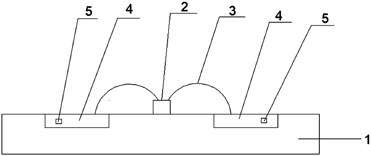
[0024] Such as figure 2 As shown, the present invention proposes a packaging structure for radio frequency microwave power amplifier devices, including a GaN radio frequency power amplifier chip 2, a ceramic circuit board 4, a copper-containing metal substrate 1 and a passive device 5, and the GaN radio frequency power amplifier chip 2 is arranged on a copper-containing On the metal substrate 1, the passive device 5 is arranged on the ceramic circuit board 4, the GaN radio frequency power amplifier chip 2 is electrically connected to the ceramic circuit board 4 through the copper wire 3, and the inner surface of the copper-containing metal substrate 1 is provided with a first groove and a second groove. Two grooves, the ceramic circuit board 4 is fixedly arranged in the first groove and the second groove, and the passive device 5 is one or more of capacitors, inductors, resistors or microstrip lines.

Embodiment 3

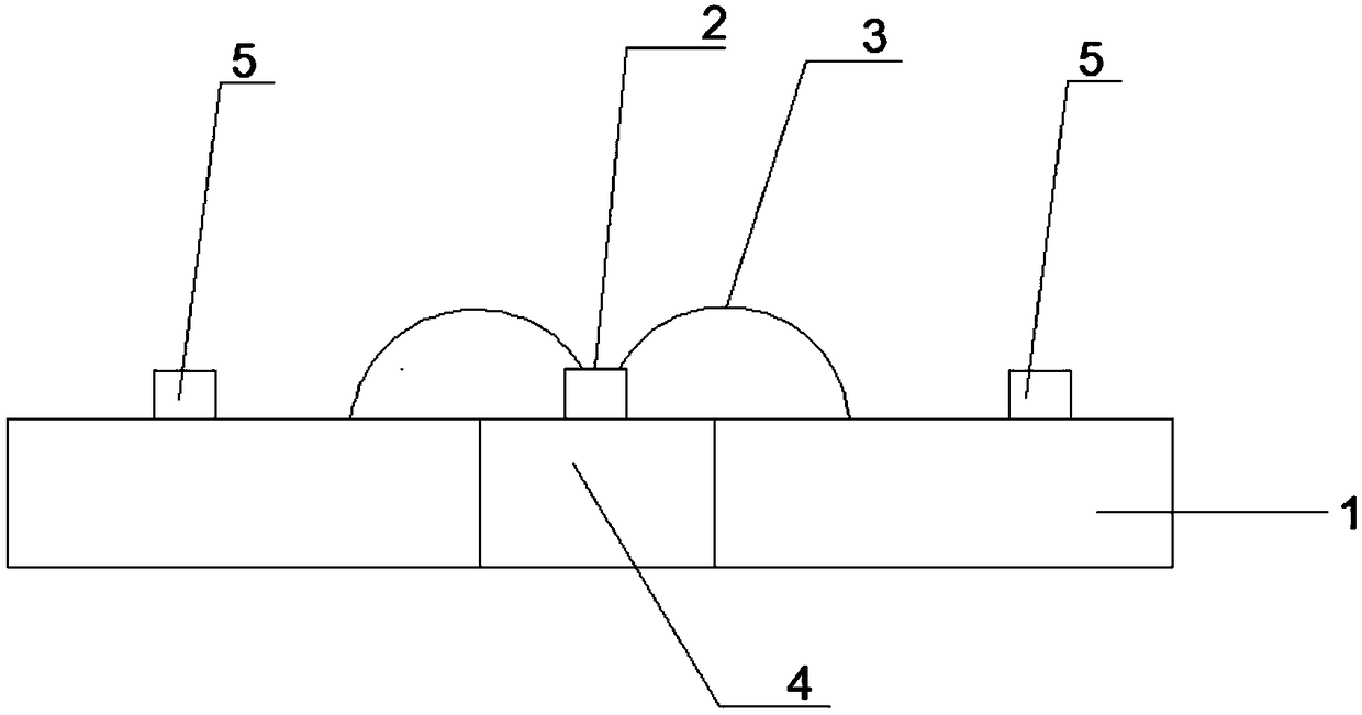
[0026] Such as image 3 As shown, the present invention proposes a packaging structure for radio frequency microwave power amplifier devices, including a PCB circuit board 1, a GaN radio frequency power amplifier chip 2, a copper substrate 4 and a passive device 5, and the GaN radio frequency power amplifier chip 2 is arranged on the copper substrate 4 , the passive device 5 is arranged on the PCB circuit board 1, the GaN radio frequency power amplifier chip 2 is electrically connected to the PCB circuit board 1 through the gold wire 3, the PCB circuit board 1 is provided with a cavity, and the copper substrate 4 is embedded in the cavity, without The source device 5 is one or more of capacitors, inductors, resistors or microstrip lines.

[0027] By adopting PCB circuit board, opening a hole in the middle of PCB circuit board, embedding copper substrate to improve the heat dissipation capability of GaN RF power amplifier chip, passive components connect the circuit through PCB...


PUM


Abstract

The invention relates to a packaging structure for an RF microwave power amplifier. The packaging structure comprises an RF power amplification chip, a circuit substrate, a metal substrate and a passive device, the RF power amplification chip is arranged on the metal substrate, the passive device is arranged on the circuit substrate, the metal substation is combined with the circuit substrate in asplicing manner, and the metal power amplification chip is connected to the circuit substrate via a metal connecting line. A high-heat-conduction metal material serves as the metal substrate, so thatthe heat radiation effect of the RF power amplification chip is improved; the RF power amplification chip and the passive device are arranged on the metal substrate and the circuit substrate respectively, the metal substation is combined with the circuit substrate in the splicing manner, thus, a resistor, inductor, capacitor or microstrip line with a relatively high Q value in the market can be used more conveniently, the research and development period is shortened, the cost is lower, and performance and reliability of a product are ensured; and design requirement can be reached via parameter adjustment of products as the resistor, inductor, capacitor and microstrip line, and the flexibility is high.

Description

technical field [0001] The invention relates to the technical field of semiconductors, in particular to a packaging structure for radio frequency microwave power amplifier devices. Background technique [0002] Power amplifiers based on radio frequency microwaves have been widely used in designs such as monolithic microwave integrated circuits (MMICs) and hybrid integrated circuits (HICs). Although the MMIC RF power amplifier chip is small in size and has good consistency, it needs to integrate passive devices such as resistors, capacitors, and inductors on the RF power amplifier chip of the power amplifier, resulting in a large area of ​​the RF power amplifier chip and high cost. It is usually suitable for applications above millimeter wave, or application scenarios with ultra-high performance requirements. Although HIC in the form of a module has low R&D difficulty and low cost, the circuit composition of the internal module is complex, requiring at least 3 kinds of compo...

Claims


Application Information

Patent Timeline
Patent Type & Authority Applications(China)
IPC IPC(8): H01L23/14H01L23/367H01L23/373H01L25/16
CPCH01L2224/48091H01L2924/00014H01L25/165H01L23/14H01L23/3672H01L23/3736
Inventor 张达泉杨荣张昊孙丞
Owner 苏州本然微电子有限公司
Why Eureka
Try Eureka