Packaging structure and manufacturing method thereof

A technology of packaging structure and manufacturing method, which is applied in semiconductor/solid-state device manufacturing, electrical components, electrical solid-state devices, etc., to achieve the effects of reducing manufacturing costs, reducing thickness, and ensuring simplicity

Inactive Publication Date: 2018-11-13
POWERTECH TECHNOLOGY
View PDF5 Cites 2 Cited by
  • Summary
  • Abstract
  • Description
  • Claims
  • Application Information

AI Technical Summary

Problems solved by technology

Therefore, miniaturizing the package structure while maintaining process simplification has become a major challenge for those skilled in the art.

Method used


Image

  • Packaging structure and manufacturing method thereof
  • Packaging structure and manufacturing method thereof
  • Packaging structure and manufacturing method thereof

Examples


Embodiment Construction

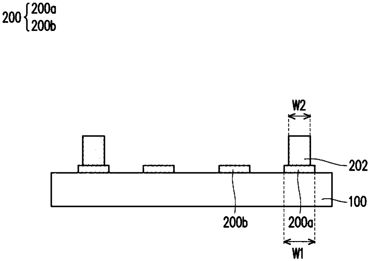
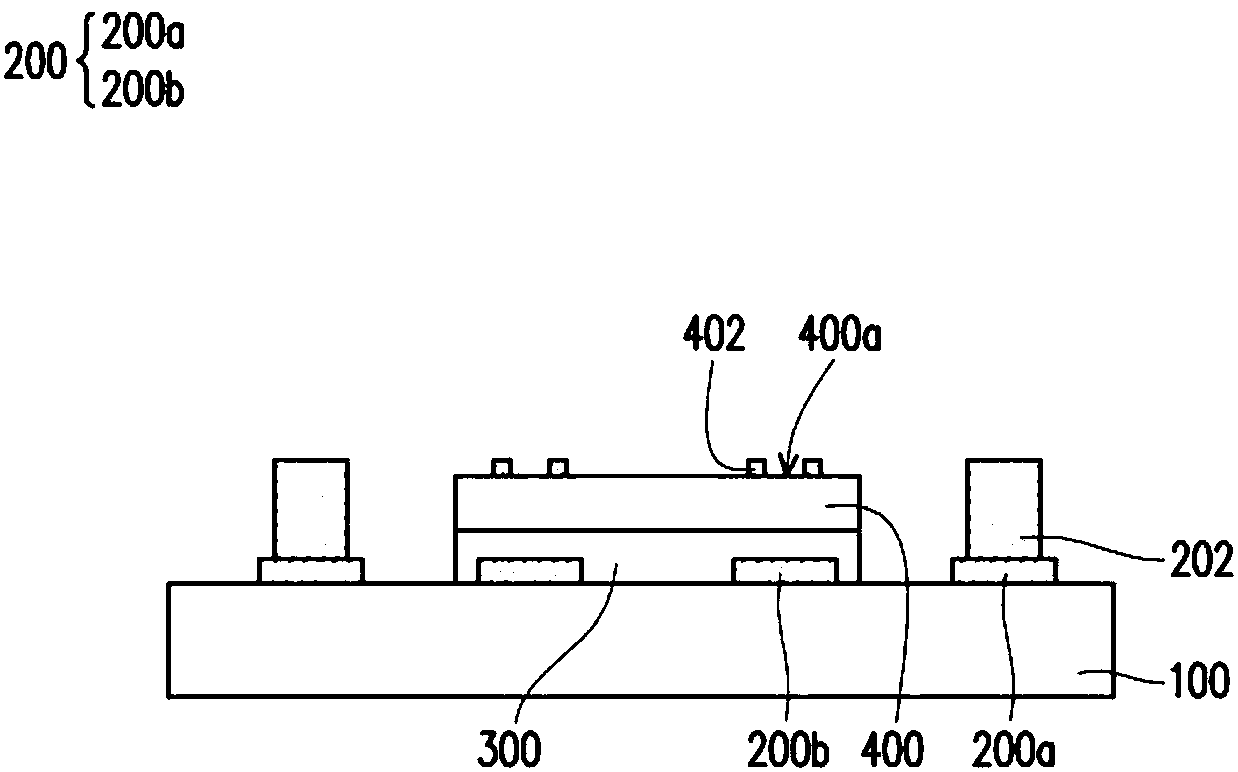
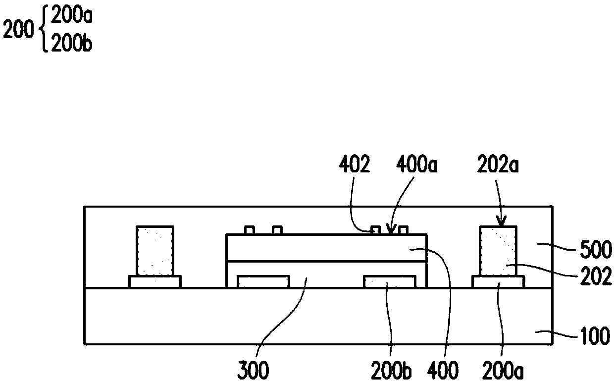
[0038] Figure 1A to Figure 1J It is a schematic cross-sectional view of the manufacturing process of the packaging structure 10 according to an embodiment of the present invention.

[0039] refer to Figure 1A , providing a carrier substrate 100 . The carrier substrate 100 includes a metal carrier substrate, a glass carrier substrate or a silicon wafer substrate. For example, in this embodiment, a metal carrier substrate can be used as the carrier substrate 100 . Other materials of the carrier substrate utilized in other embodiments may also be used in this embodiment. A first circuit layer 200 is formed on the carrier substrate 100 . In some embodiments, the formation of the first circuit layer 200 on the carrier substrate 100 may be performed by, for example, an electroless plating process, a chemical plating process, a thermal evaporation process or sputtering. Process (sputtering process). For example, a metal layer (not shown) can be formed on the carrier substrate ...


PUM


Abstract

The invention provides a packaging structure and a manufacturing method thereof. The packaging structure includes an insulating sealing body, an adhesive layer, a first circuit layer, a chip, a plurality of conductive structures, a dielectric layer and a second circuit layer. The insulating sealing body has a first surface and a second surface. The adhesive layer, the chip, the conductive structures and at least part of the first circuit layer are embedded in the insulating sealing body. In addition, at least part of the first circuit layer is embedded in the adhesive layer. The first circuitlayer includes a plurality of first connection pads and a plurality of second connection pads. The chip including a plurality of connection terminals is arranged on the adhesive layer. The conductivestructures are electrically connected to the first connection pads. The dielectric layer is arranged on the second surface of the insulating sealing body. The second circuit layer is electrically connected to the conductive structures and the connection terminals.

Description

technical field [0001] The present invention relates to a packaging structure and a manufacturing method thereof, in particular to a packaging structure with a molded interconnect substrate (MIS) formed therein and a manufacturing method thereof. Background technique [0002] In order to make the design of electronic products thinner and smaller, the semiconductor packaging technology is also advancing day by day to develop products that meet the requirements of small size, light weight, high density and high competitiveness in the market. Therefore, miniaturization of the packaging structure while maintaining a simplified process has become a major challenge for those skilled in the art. Contents of the invention [0003] The invention provides a packaging structure and a manufacturing method thereof, which can effectively reduce its size and manufacturing cost. [0004] The invention provides a packaging structure. The packaging structure includes an insulating sealing...

Claims


Application Information

Patent Timeline
IPC IPC(8): H01L23/488H01L23/31H01L21/56H01L21/60
Inventor 徐宏欣陈裕纬
Owner POWERTECH TECHNOLOGY
Why Eureka
Try Eureka