
Monolithic n-i-p-i-n type wide-spectrum photodetector

A technology of n-i-p-i-n and photodetectors, which is applied in circuits, electrical components, semiconductor devices, etc., can solve the problems of quantum efficiency decline, affecting detection sensitivity and spectral response range, etc., and achieve quantum efficiency improvement, detection sensitivity improvement, and dark current reduction Effect

Active Publication Date: 2018-11-13
HANGZHOU GUOYI TECH CO LTD
View PDF7 Cites 7 Cited by
  • Summary
  • Abstract
  • Description
  • Claims
  • Application Information

AI Technical Summary

Problems solved by technology

For the extended short-wave infrared InGaAs detector with a response cutoff wavelength greater than 1.7 μm, due to the absorption of the narrow bandgap lattice mismatch buffer layer or the contact top layer (back-incidence or front-illumination), the quantum efficiency in the short-wavelength direction decreases significantly, affecting To improve the detection sensitivity and spectral response range; when the response cut-off wavelength extends to 2.5 μm, the response turn-on wavelength is greater than 1.2 μm, and the quantum efficiency below 1.5 μm wavelength is usually lower than 30%, how to improve the detection sensitivity of InGaAs detectors below 1.7 μm wavelength It is a technical problem that needs to be solved urgently

Method used


Image

  • Monolithic n-i-p-i-n type wide-spectrum photodetector
  • Monolithic n-i-p-i-n type wide-spectrum photodetector
  • Monolithic n-i-p-i-n type wide-spectrum photodetector

Examples


Embodiment Construction

[0026] Embodiments of the present invention are described in detail below, examples of which are shown in the drawings, wherein the same or similar reference numerals designate the same or similar elements or elements having the same or similar functions throughout. The embodiments described below by referring to the figures are exemplary only for explaining the present invention and should not be construed as limiting the present invention.

[0027] In describing the present invention, it should be understood that the terms "longitudinal", "transverse", "upper", "lower", "front", "rear", "left", "right", "vertical", The orientation or positional relationship indicated by "horizontal", "top", "bottom", "inner", "outer", etc. are based on the orientation or positional relationship shown in the drawings, and are only for the convenience of describing the present invention and simplifying the description, rather than Nothing indicating or implying that a referenced device or elem...


PUM


Abstract

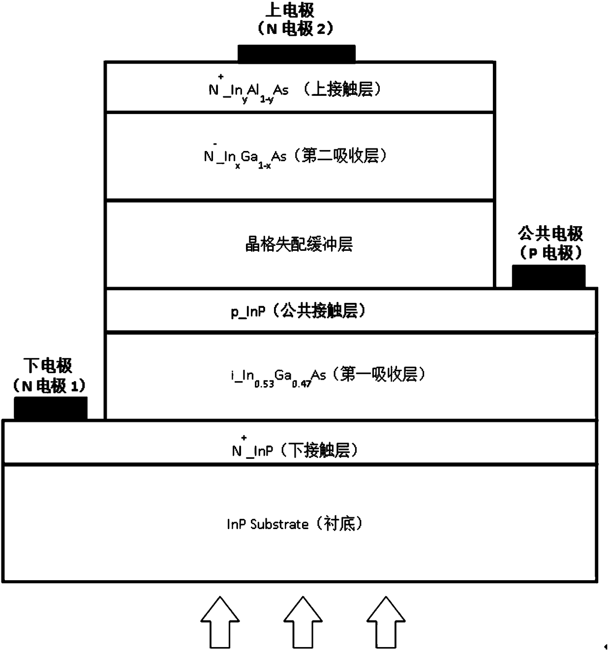
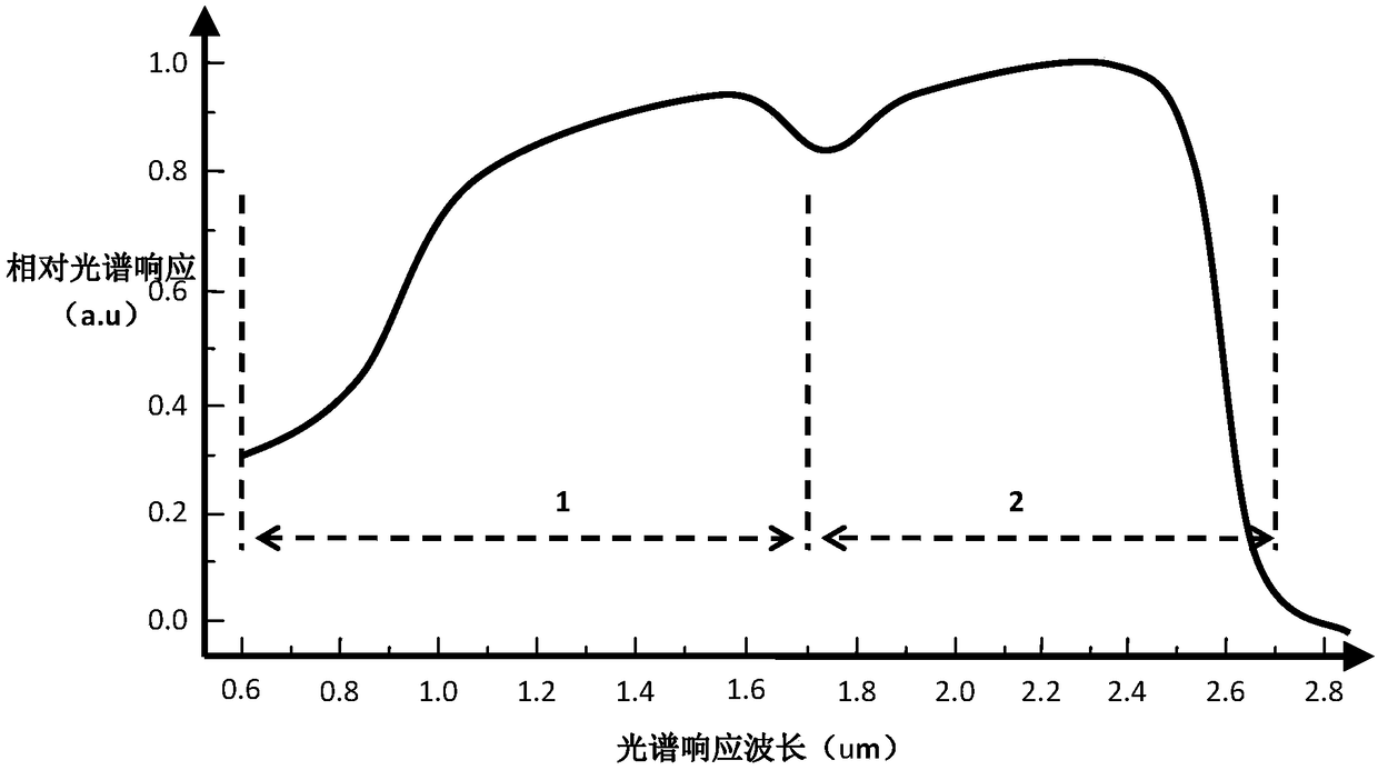
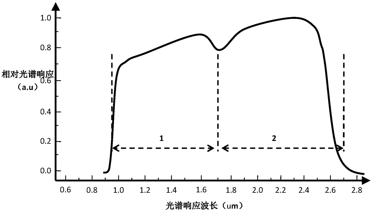
The invention provides a monolithic n-i-p-i-n type wide-spectrum photodetector including an InP substrate; an InP of a first conductivity type as a lower contact layer on the InP substrate is formed;an intrinsic Inx1Ga1-x1As as the first absorption layer is formed over the lower contact layer; a second conductive type InP as a common contact layer is formed over the first absorbing layer; a lattice adapted buffer lay is formed over common contact layer; Inx2Ga1-2As of intrinsic or first conductivity class is formed over the lattice adaptation buffer layer; a first conductivity type Inx3Al1-x3As upper contact layer is formed on a second absorption layer. A PIN detector with standard wavelength response and a PIN detector with extended wavelength response are combined by adopting a two-color detector design scheme, and PD1 is used to respond to a spectrum range below 1.7 mum, PD2 is used to respond to a spectrum range of 1.7 mum-2.5 mum. PD1 and PD2 share a P electrode to form a back incident n-i-p-i-n type device structure, and the modulation of the response spectrum by switching the electrode bias is realized.

Description

technical field [0001] The invention belongs to the technical field of semiconductor design and manufacture, relates to the technical field of InP-based III-V compound semiconductor optoelectronic devices, and specifically relates to a single-chip n-i-p-i-n type wide-spectrum photodetector with a novel structure. Background technique [0002] The "near-infrared-short-wave infrared" (0.75-2.5μm) spectrum band is the most important band range for spectral sensing detection and spectral analysis applications, and has application requirements in the fields of industry, communication, medical treatment, food, biochemistry, agriculture, and public safety. widely. At present, in this spectral range, InGaAs and HgCdTe are the most mainstream detector technologies. [0003] In recent years, with the continuous progress of material preparation technology, emerging detector technologies such as type-II superlattice (T2SL) and colloidal quantum dots (CQD) have also developed rapidly. ...

Claims


Application Information

Patent Timeline
IPC IPC(8): H01L31/105H01L31/115H01L31/18
CPCH01L31/105H01L31/115H01L31/1844Y02P70/50
Inventor 邹泽亚
Owner HANGZHOU GUOYI TECH CO LTD
Learn More