

A device and method for measuring thermal conductivity of thin films based on mems technology
A test device and thermal conductivity technology, applied in the field of micro-electromechanical system devices, can solve the problems of complex and expensive system construction, without considering thermal conductivity measurement, etc., to achieve mature and reliable, clear principle, and reduce radiation heat dissipation
- Summary
- Abstract
- Description
- Claims
- Application Information
AI Technical Summary
Problems solved by technology
Method used
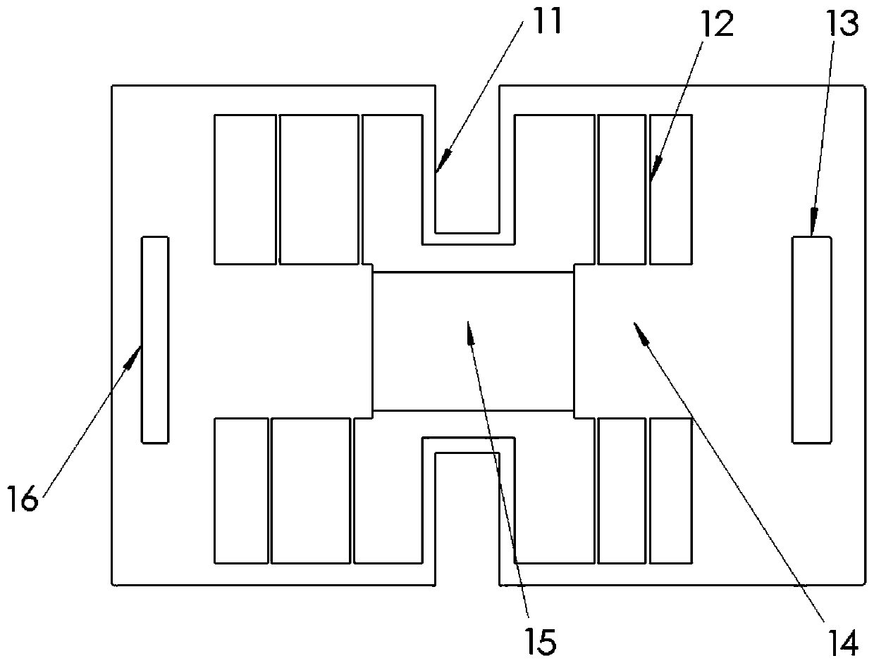
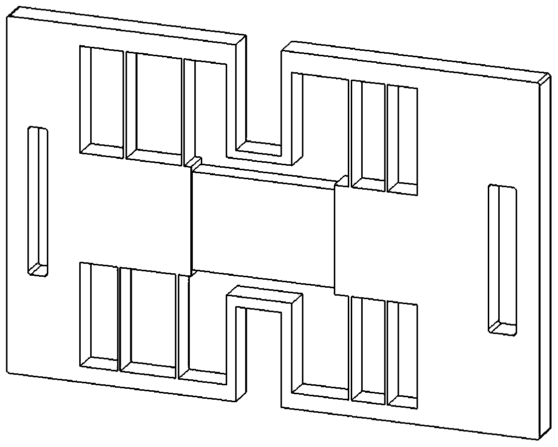
Image

Examples
Embodiment Construction
[0037] The present invention will be described in detail below in conjunction with the accompanying drawings and specific embodiments, where the schematic embodiments and descriptions of the present invention are used to explain the present invention, but not to limit the present invention.
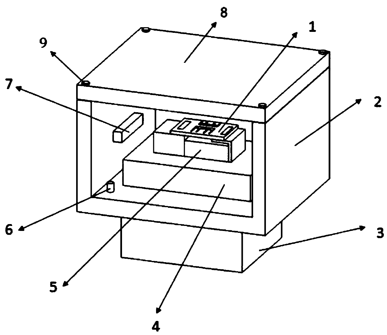
[0038] like figure 1 As shown, the MEMS technology-based film strain thermal conductivity testing device of the present invention includes an outer shield 2, and a heating platform 3 is provided below the outer shield 2 for supporting the shield body and placing heating components. 2 is provided with a stage 4, and the way of placing the stage in the shielding cover can be to connect with a slot on the stage or to stick it directly. A piezoelectric test device 5 is provided on the stage 4, and a test piece 1 is placed on the piezoelectric test device 5; a temperature sensor 7 and a vent hole 6 are provided on the inner wall of the outer shield 2.
[0039] The external shield of the devic...
PUM
| Property | Measurement | Unit |
|---|---|---|
| thickness | aaaaa | aaaaa |
Abstract
Description
Claims
Application Information