

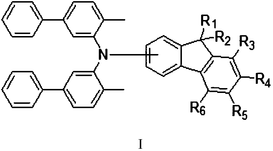
Compound based on biphenylamine and application thereof as well as organic electroluminescent device
A dibenzidine and compound technology, applied in the field of organic electroluminescent materials, can solve the problems of high preparation energy consumption, affect device efficiency, poor thermal stability, etc., and achieve high luminous efficiency, high luminous purity, and good thermal stability. Effect
- Summary
- Abstract
- Description
- Claims
- Application Information
AI Technical Summary
Problems solved by technology
Method used
Image

Examples
Embodiment 1
[0045] Synthetic route of compound 4
[0046]
[0047] The synthetic method of compound 4
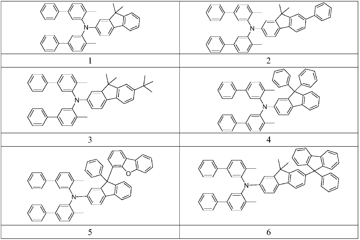
[0048] In the flask, add 4-methyl-N-(4-methyl[1,1'-biphenyl]-3-yl)-[1,1'-biphenyl]-3-amine (3g, 8.6mmol), 9,9-diphenyl-2-bromofluorene (3.4g, 8.6mmol), sodium tert-butoxide (2g, 20mmol), palladium acetate (0.1g), X-phos (0.3g), toluene (30 mL), heated to reflux under nitrogen protection for 5 hours, cooled, and the solvent was removed. The crude product was purified by column chromatography to obtain 4.5 g with a yield of 79%.
[0049] The synthesis method of other examples is consistent with that of compound 4, all of which use diphenylidine as a raw material, and then react with other brominated compounds, as shown in Table 1 below:
[0050] Table 1
[0051]
Embodiment 6-10
[0053] Fabrication of Organic Electroluminescent Devices
[0054] Preparation of OLEDs using the compounds of the Examples
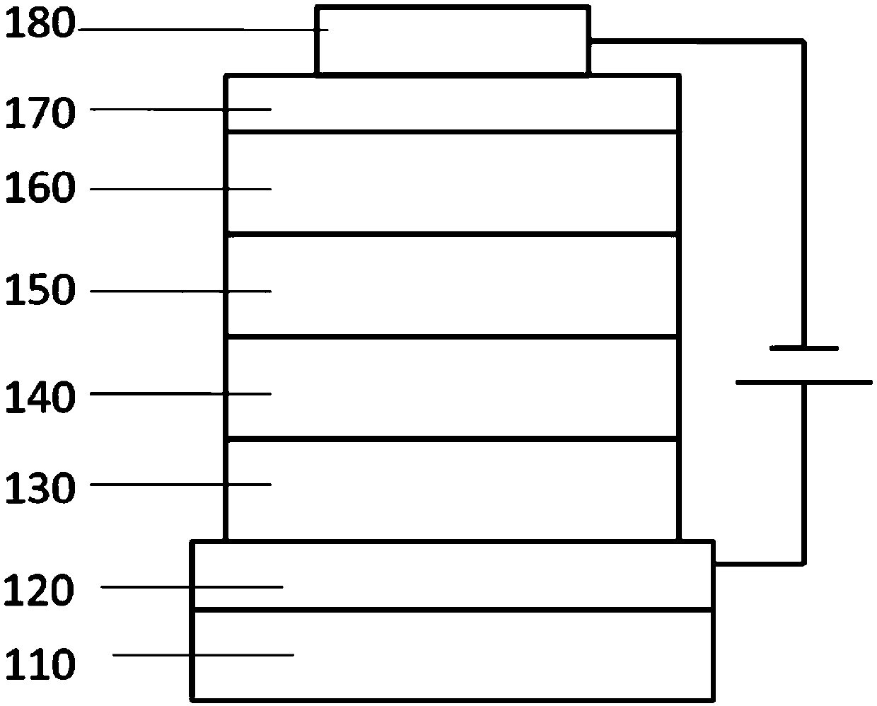
[0055] First, the transparent conductive ITO glass substrate 110 (with anode 120 on it) (China CSG Group Co., Ltd.) is washed in sequence with deionized water, ethanol, acetone and deionized water, and then treated with oxygen plasma for 30 seconds.
[0056] Then, PEDOT:PSS (polyethylenedioxythiophene-poly(styrene sulfonate)) with a thickness of 45 nm was spin-coated on the ITO as the hole injection layer 130, and dried at 150° C. for 30 minutes.
[0057] Then, the compound of the present invention was vapor-deposited as the hole transport material 140 on the hole injection layer to a thickness of 40 nm.
[0058] Then, a luminescent layer 150 with a thickness of 30nm is evaporated on the electron blocking layer, wherein CBP is the host luminescent material, and the weight ratio is 8% of Ir(ppy) 3 As a phosphorescent doping guest material.
[0059] The...
PUM
 Abstract
Description
Claims
Application Information