Wireless transmission module and manufacturing method thereof

A wireless transmission and module technology, which is applied in transmission systems, semiconductor/solid-state device manufacturing, electrical components, etc., can solve the disadvantages of miniaturization and thinning of electronic equipment, low integration of wireless transmission modules, and reduction of module power density and other issues, to achieve the effect of improving continuous normal working ability, facilitating heat dissipation, and improving miniaturization and thinning

Active Publication Date: 2018-11-27
HUAWEI TECH CO LTD
View PDF5 Cites 2 Cited by
  • Summary
  • Abstract
  • Description
  • Claims
  • Application Information

AI Technical Summary

Problems solved by technology

like figure 1 As shown, the chip 11 and the passive components 12 are mounted on the main board 13 of the electronic device, and the coil and the magnetic material 14 are arranged outside the main board 13 (generally arranged near the position of the complete machine shell of the electronic device), thus, the wireless transmission mode The coil of the group is separated from the chip 11, resulting in low integration of the wireless transmission module
In the wireless transmission module with a low integration level, both the chip 11 and the passive components 12 need to be mounted on the main board 13, resulting in the wireless transmission module occupying a large area of ​​the main board 13 of the electronic equipment, which is not conducive to electronic equipment. miniaturization and thinning
[0004] In addition, the sensitive components in the wireless transmission module, such as the chip 11 and the passive components 12, are directly mounted on the motherboard of the electronic device, so the sensitive components are exposed to the external environment and are easily damaged, making the product reliable. lower sex
[0005] Moreover, the chip 11 is separated from the coil, and the circuit path is relatively long, which will generate a large parasitic impedance
And larger parasitic impedance will reduce the power density of the module

Method used


Image

  • Wireless transmission module and manufacturing method thereof
  • Wireless transmission module and manufacturing method thereof
  • Wireless transmission module and manufacturing method thereof

Examples


Embodiment Construction

[0058] Based on the background technology part, it can be seen that the existing wireless transmission module has the problem of low integration, and further has the following problems:

[0059] 1) It is not conducive to the miniaturization and thinning of electronic equipment assembled with wireless transmission modules;

[0060] 2) The sensitive components in the wireless transmission module are easily damaged, and the product reliability is low;

[0061] 3) There is a large family planning impedance, which makes the power density of the module low.

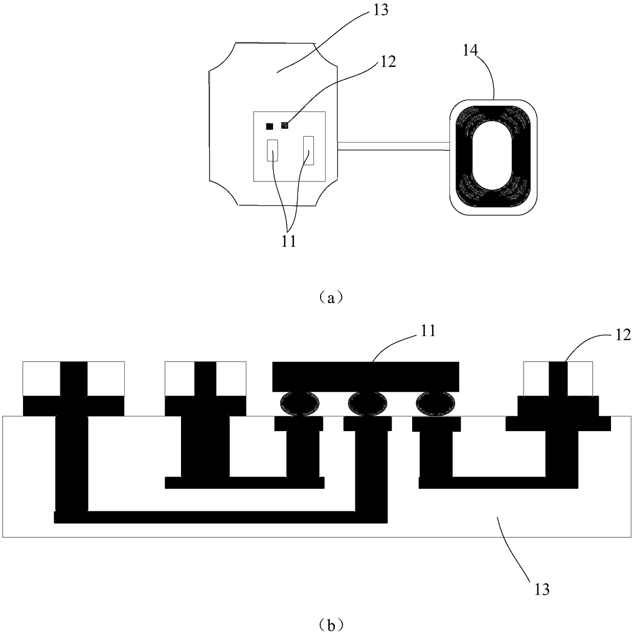
[0062] In order to solve the above technical problems, the embodiment of the present application integrates the chip, passive components, magnetic materials and coils to form a wireless transmission module with an integrated structure, so as to improve the integration degree of the wireless transmission module. The wireless transmission module with integrated structure can be flexibly arranged inside the whole electronic devic...


PUM


Abstract

The application discloses a wireless transmission module and a manufacturing method thereof. The wireless transmission module has an integrated structure formed by a chip, a passive component and a coil, so that the integration degree of the wireless transmission module is improved. Moreover, on the basis of the integrated structure, the independence of the module can be realized effectively; flexible layout inside the electronic device is realized by using the independent module; and because only the input terminal of the wireless transmission module needs to be kept on the main board of theelectronic device instead of setting the independent module on the main board of the electronic device, the board occupation area by the wireless transmission module is reduced. Besides, on the basisof the wireless transmission module, the continuous normal working capability of the product in an extreme condition scene can be enhanced effectively and the product reliability is improved. In addition, the chip and the coil are integrated into one in the wireless transmission module and thus the signal transmission path between the chip and the coil is short, so that the generated parasitic impedance is small.

Description

technical field [0001] The present application relates to the technical field of semiconductor manufacturing, in particular to a wireless transmission module and a manufacturing method. Background technique [0002] Wireless charging, NFC (Near Field Communication, short-range wireless communication technology) and other wireless transmission modules use electromagnetic fields to transmit signals / energy between transmitters and receivers, and are widely used in various types of electronic devices. [0003] At present, an assembly structure of wireless transmission modules and electronic equipment is as follows: figure 1 , where (a) is a top view of the assembly structure, and (b) is a schematic cross-sectional view of the assembly structure. Such as figure 1 As shown, the chip 11 and the passive components 12 are mounted on the main board 13 of the electronic device, and the coil and the magnetic material 14 are arranged outside the main board 13 (generally arranged near t...

Claims


Application Information

Patent Timeline
Patent Type & Authority Applications(China)
IPC IPC(8): H04B1/40
CPCH04B1/40H01L2924/19105H01L2224/04105H01L2224/24137H01L2224/24195H01L2224/96H01L2924/3025H04B1/03H04B1/04H01L21/56H01L23/552H01L23/66H01L24/24H01L24/82H01L25/16H01L2223/6677H01L2224/24011H01L2224/24101H01L2224/82101H01L2224/82106
Inventor 何气敬廖小景侯召政
Owner HUAWEI TECH CO LTD
Why Eureka
Try Eureka