Broadband perfect absorber based on metallic film-core shell plasma structure

A plasma and perfect absorption technology, which is applied in the field of perfect absorption materials and its preparation, can solve the problems of high cost and cumbersome process, and achieve the effects of low production cost, controllable area and simple structure

Active Publication Date: 2018-11-30
THE NAT CENT FOR NANOSCI & TECH NCNST OF CHINA
View PDF12 Cites 16 Cited by
  • Summary
  • Abstract
  • Description
  • Claims
  • Application Information

AI Technical Summary

Problems solved by technology

Recently, broadband plasmonic absorbers have been reported, most of which have a sandwich structure, that is, metal-dielectric layer (semicon

Method used


Image

  • Broadband perfect absorber based on metallic film-core shell plasma structure
  • Broadband perfect absorber based on metallic film-core shell plasma structure
  • Broadband perfect absorber based on metallic film-core shell plasma structure

Examples


preparation example Construction

[0043] In order to achieve the above object, the present invention also provides a method for manufacturing a broadband perfect absorber based on a metal thin film-core-shell plasma structure. Preferably, the preparation method specifically includes:

[0044] Prepare a chromium film layer on the base ITO;

[0045] Physically depositing a gold film layer on the chromium film layer;

[0046] Deposit a layer of Au@Cu on the upper surface of the gold film layer by liquid-liquid self-assembly method 2 O granular layer;

[0047] Deposit a layer of Au@Cu on the upper surface of the gold film layer by liquid-liquid self-assembly method 2 O granular layer.

Embodiment 1

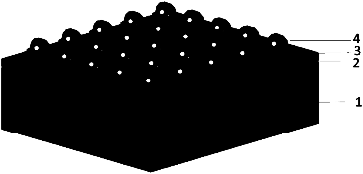
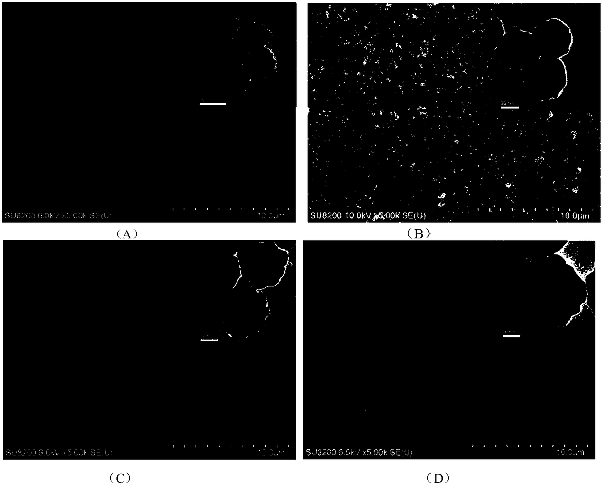
[0050] A broadband perfect absorber based on a metal thin film-core-shell plasma structure, including a substrate, the material of the substrate is ITO, and the substrate 1 is sequentially provided with a chromium film layer, a gold film layer and Au@Cu 2 O structural layer. In this embodiment, the diameter of the core of the core-shell structure is 20 nanometers, and the diameter of the core-shell structure is 50 nanometers (see figure 2 (A)), the core-shell structure film layer is a single layer of Au@Cu 2 O plasmonic nanoparticle core-shell structure particle composition.

[0051] The preparation method of this perfect absorber is:

[0052] A chromium film layer is prepared by vapor deposition on the base ITO, with a thickness of 10 nanometers;

[0053] Physically deposit a gold film layer on the chromium film layer with a thickness of 100 nanometers;

[0054] Deposit a layer of Au@Cu on the upper surface of the gold film layer by liquid-liquid self-assembly method 2 ...

Embodiment 2

[0061] A broadband perfect absorber based on a metal thin film-core-shell plasma structure, including a substrate, the material of the substrate is ITO, and the substrate 1 is sequentially provided with a chromium film layer, a gold film layer and Au@Cu 2 O structural layer. In this embodiment, the diameter of the core of the core-shell structure is 35 nanometers, and the diameter of the core-shell structure is 50-100 nanometers (see figure 2 (B)), the core-shell structure thin film layer is a single layer of Au@Cu 2 O plasmonic nanoparticle core-shell structure particle composition. The preparation process is:

[0062] Preparation of 35nm gold particles: Add 28mL of 20nm gold particles (preparation method is the same as in Example 1) into 75mL of water as gold seed sol, under vigorous stirring, add 0.56mL of 0.2mol / L hydroxylamine hydrochloride solution, and finally add 1mL of 1% Chlorauric acid solution, continue to stir for 30min.

[0063] Au@Cu 2 Preparation of O: 1 ...


PUM

PropertyMeasurementUnit
Thicknessaaaaaaaaaa
Thicknessaaaaaaaaaa
Diameteraaaaaaaaaa

Abstract

The invention provides a broadband perfect absorber based on a metallic film-core shell plasma structure. The broadband perfect absorber comprises a substrate, the broadband perfect absorber is of a multi-layered structure arranged on the substrate, a metallic film layer and a core shell nano-particle film layer are sequentially arranged from the substrate up, the core shell nano-particle film layer is composed of core shell particles with local surface plasma resonance characteristics, and the core shell particles are constituted by taking precious metals as cores and semiconductors as shells. The invention further provides a preparation method of the broadband perfect absorber. The broadband perfect absorber is simple in structure and optional in substrate, the metallic film can be a gold thin film, a silver thin film, a copper thin film and the like, liquid-liquid interface is used for self-assembling into a film, the operation is convenient, the area is controllable, the broadbandperfect absorber is suitable for a plurality of compounds of the precious metals and the semiconductors, and the manufacturing cost is low.

Description

technical field [0001] The invention belongs to the field of optical materials, and in particular relates to a perfect absorption material and a preparation method thereof. Background technique [0002] The absorption efficiency of light is the core issue of some devices, such as solar cells, photodetectors, imaging sensors, biosensors, etc., but natural materials have weak absorption or strong reflection, and poor response in the visible spectrum range, with metal Perfect absorbers of elements have been fabricated, such as: porous metal films; grating structure systems and metamaterials, etc., through the phenomenon of electromagnetic resonance, the structure has neither reflection (reflectivity close to 0) nor transmission (transmittance) at the resonant wavelength. is 0), so that according to the definition of absorption A=1-R-T (wherein A represents the absorptivity, R represents the reflectivity, and T represents the transmittance), the perfect absorption with the absor...

Claims


Application Information

Patent Timeline
IPC IPC(8): G02B5/00G02B1/00
CPCG02B1/002G02B5/003
Inventor 王晓莉李洪东唐智勇
Owner THE NAT CENT FOR NANOSCI & TECH NCNST OF CHINA
Why Eureka
Try Eureka