Electron beam exposure method, electron beam lithography method and metal line preparation method
A technology of electron beam exposure and electron beam lithography, which is applied in the field of semiconductors, can solve the problems of uneven electron beam exposure and achieve the effect of small line size
- Summary
- Abstract
- Description
- Claims
- Application Information
AI Technical Summary
Problems solved by technology
Method used
Image

Examples
Embodiment 1
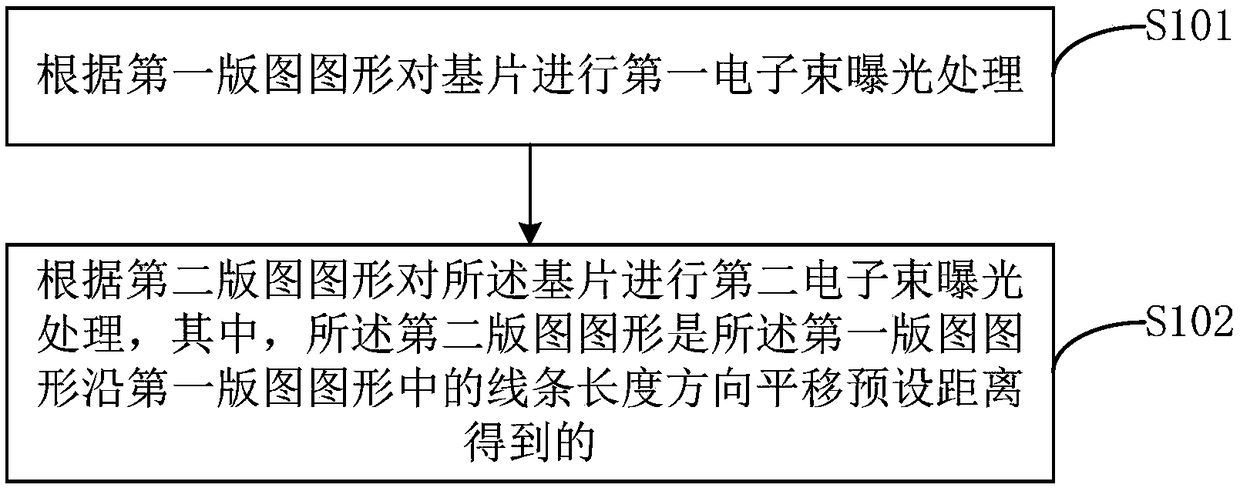
[0037] Please refer to figure 1 , figure 1 It is a schematic diagram of the implementation flow of the electron beam exposure method provided in Embodiment 1 of the present invention, and the method includes the following steps:
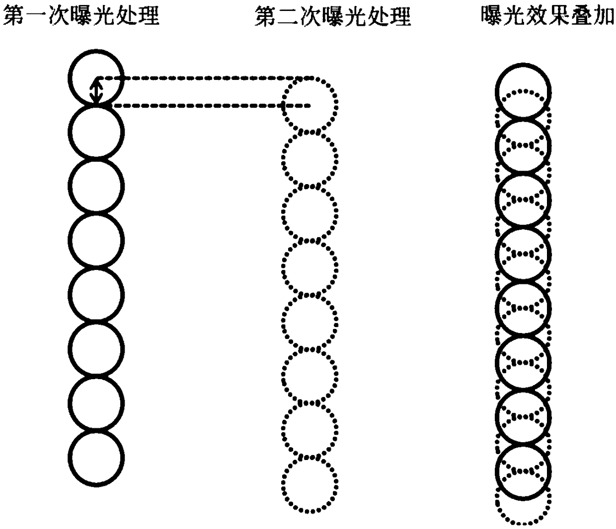
[0038] Step S101, performing a first electron beam exposure treatment on the substrate according to the first layout pattern.
[0039] In the embodiment of the present invention, L-Edit software is used to design the first layout pattern, wherein the line size of at least one line in the first layout pattern, that is, the line width, is the beam spot diameter of the electron beam. For example, if the electron beam spot diameter is 10 nanometers, then the line width of at least one line in the first layout pattern is 10 nanometers. Using an exposure machine to perform a first electron beam exposure treatment on the substrate according to the first layout pattern.
[0040] Step S102, performing a second electron beam exposure process on the substrat...
Embodiment 2
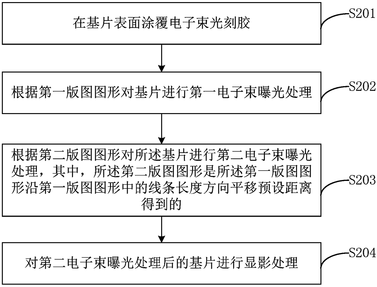
[0050] Please refer to image 3 , image 3 It is a schematic diagram of the implementation flow of the electron beam lithography method provided in Embodiment 2 of the present invention, and the method includes the following steps:
[0051] Step S201, coating electron beam photoresist on the surface of the substrate.
[0052] In an embodiment of the present invention, the electron beam photoresist is spin-coated on the surface of the substrate, wherein the rotation speed in the spin coating is 2000 rpm to 5000 rpm, and a hot plate of 160 to 190 degrees Celsius is used to bake the glue 2 minutes to 5 minutes. The e-beam photoresist can be PMMA, type C2.
[0053] Step S202, performing a first electron beam exposure treatment on the substrate according to the first layout pattern.
[0054] Step S203, performing a second electron beam exposure process on the substrate according to the second layout pattern, wherein the second layout pattern is the first layout pattern shifted ...
Embodiment 3
[0060] Please refer to Figure 4 , Figure 4 It is a schematic flow chart of the method for preparing a metal wire provided in Embodiment 3 of the present invention, and the method includes the following steps:
[0061] Step S301, coating electron beam photoresist on the surface of the substrate.
[0062] Step S302, performing a first electron beam exposure treatment on the substrate according to the first layout pattern.
[0063] Step S303, performing a second electron beam exposure process on the substrate according to the second layout pattern, wherein the second layout pattern is the first layout pattern shifted by a preset distance along the line length direction of the first layout pattern owned.
[0064] Step S304, developing the substrate after the second electron beam exposure treatment.
[0065] The implementation manner of step S301 to step S301 is the same as the implementation manner of step S201 to step S204 in the second embodiment of the present invention, ...
PUM
| Property | Measurement | Unit |
|---|---|---|
| thickness | aaaaa | aaaaa |
| thickness | aaaaa | aaaaa |
Abstract
Description
Claims
Application Information