Multi-index detection device based on localized surface plasmon resonance sensing
A plasma resonance and localized surface technology, applied in instruments, measuring devices, scientific instruments, etc., can solve problems such as mobile medical care, remote monitoring and food hygiene source monitoring, single sensor detection index, and inconvenient integration of detection terminals. , to achieve the effect of improving test efficiency, improving detection efficiency, and high integration
- Summary
- Abstract
- Description
- Claims
- Application Information
AI Technical Summary
Problems solved by technology
Method used
Image
Examples
Embodiment 1
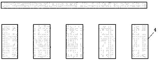
[0041] like image 3 and Figure 4 As shown, this embodiment provides a multi-index detection device based on local surface plasmon resonance sensing, including a first soft rubber layer 2, a second soft rubber layer 6, a light source 1, an ordered LSPR sensor 3, a micro The fluidic chip 4 and the signal detection element 5, the first soft rubber layer 2 is provided with a number of first installation holes, the light source 1 is installed in the first installation hole, and the first soft rubber layer 2 is loaded in order The LSPR sensor 3 and the microfluidic chip 4, the microfluidic chip 4 is covered with a second soft rubber layer 6, and the second soft rubber layer 6 is provided with a second mounting hole corresponding to the position of the first mounting hole , the signal detection element 5 is installed in the second installation hole. Wherein, the light source 1 is an LED light source or an OLED light source, preferably an LED light source; the signal detection ele...
Embodiment 2
[0044] This implementation provides a method for preparing a multi-index detection device based on localized surface plasmon resonance sensing, based on a multi-index detection device based on localized surface plasmon resonance sensing in Example 1, specifically including the following steps :
[0045] S1. Preparation of ordered LSPR sensor 3;
[0046] S2. Preparation of the microfluidic chip 4;
[0047] S3. Integration of light source 1 , ordered LSPR sensor 3 , microfluidic chip 4 and signal detection element 5 .
[0048] Wherein, the step S1 includes the following sub-steps:
[0049] S11. Preparation of a structurally uniform aluminum nanocone array master by nano-indentation technology and electrochemical etching;
[0050] S12. Pour the polydimethylsiloxane (PDMS) prepolymer into the master plate, cure at 70-90 °C for 25 min-35 min, and then peel off to obtain a PDMS nano-elastic stamp. In this embodiment, the curing temperature is preferably 80 ℃, the curing time is ...
Embodiment 3
[0065] This embodiment is similar to Embodiment 2. Further, the first soft rubber layer 2 is provided with four first installation holes, and the second soft rubber layer 6 is provided with four first installation holes corresponding to the positions of the first installation holes. Two mounting holes, that is, the obtained multi-indicator detection device can simultaneously detect four indicators of the sample, which not only increases the detection channel, but also improves the throughput of biological detection.
PUM
 Abstract
Description
Claims
Application Information


