Semiconductor structure and method of forming same

A semiconductor and gas technology, applied in the direction of semiconductor devices, semiconductor/solid-state device manufacturing, transistors, etc., can solve problems such as large contact resistance, reduced operating speed of semiconductor devices, and greater impact on the performance of MOS transistors, etc., to reduce contact resistance, contact The effect of increasing the area

Inactive Publication Date: 2018-12-04
SEMICON MFG INT (SHANGHAI) CORP +1
View PDF5 Cites 0 Cited by
  • Summary
  • Abstract
  • Description
  • Claims
  • Application Information

AI Technical Summary

Problems solved by technology

In the contact resistance of the MOS transistor, due to the small area of ​​the source and the drain, the contact resistance between the conductive plug and the conductive plug is relatively large, which has a great impact on the performance of the MOS transistor and greatly reduces the operating speed of the semiconductor device.

Method used


Image

  • Semiconductor structure and method of forming same
  • Semiconductor structure and method of forming same
  • Semiconductor structure and method of forming same

Examples


Embodiment Construction

[0034] As mentioned in the background, the contact resistance between the source, the drain and the conductive plug is relatively large.

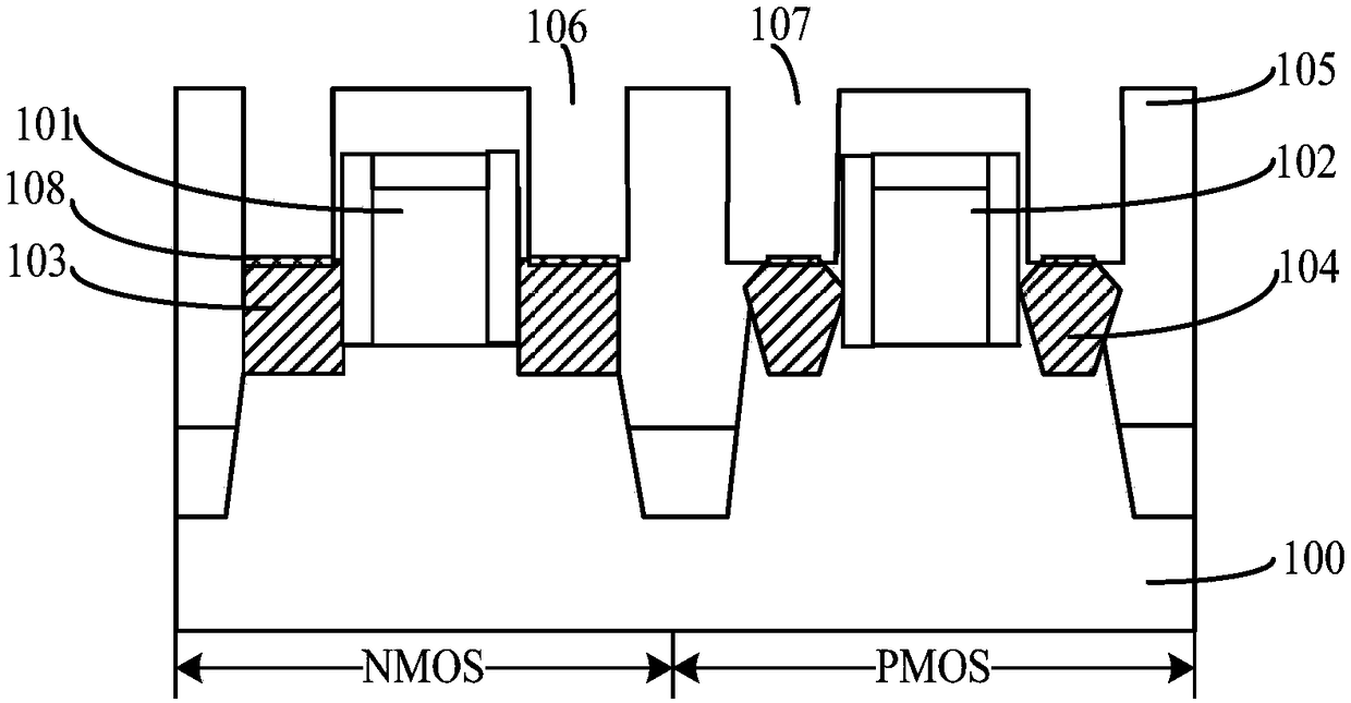
[0035] figure 1 It is a structural schematic diagram of each step of a method for forming a semiconductor structure.

[0036] Please refer to figure 1, providing the substrate 100, the substrate 100 includes an NMOS region and a PMOS region, the NMOS region substrate 100 has a first gate structure 101, the PMOS substrate 100 has a second gate structure 102, and the first The substrate 100 on both sides of a gate structure 101 has a first source-drain doped region 103, and the substrate 100 on both sides of the second gate structure 102 has a second source-drain doped region 104. The substrate 100, A dielectric layer 105 is formed on the first gate structure 101 , the second gate structure 102 , the first source-drain doped region 103 and the second source-drain doped region 104 .

[0037] Please continue to refer figure 1 , forming a fi...


PUM

PropertyMeasurementUnit
Thicknessaaaaaaaaaa

Abstract

A semiconductor structure and a method of forming the same are disclosed. The method comprises the following steps: a substrate is provided; a source / drain doping region is arranged in the substrate;a dielectric layer is arranged on the substrate and the source / drain doping region; a part, positioned on the source / drain doping region, of the dielectric layer is removed so as to form a dielectricopening; a top part surface of the source / drain doping region is exposed at a bottom part of the dielectric opening; a part, positioned on a bottom part of the dielectric opening, of a source / drain doping region is removed; a source / drain opening is formed in the source / drain doping region; metal silicide layers are formed on a sidewall and a bottom part surface of the source / drain opening; the method can help reduce contact resistance of the semiconductor device.

Description

technical field [0001] The invention relates to the field of semiconductor manufacturing, in particular to a semiconductor structure and a forming method thereof. Background technique [0002] With the continuous development of semiconductor technology, the size of semiconductor devices is continuously reduced. As the size of the semiconductor device shrinks, the contact resistance of the MOS transistor has an increasing impact on the performance of the MOS transistor and the entire semiconductor chip. In order to improve the performance of semiconductor chips, it is necessary to reduce the contact resistance of MOS transistors. In the contact resistance of the MOS transistor, due to the small area of ​​the source and the drain, the contact resistance between the conductive plug and the conductive plug is relatively large, which greatly affects the performance of the MOS transistor and greatly reduces the operating speed of the semiconductor device. [0003] Formation proc...

Claims


Application Information

Patent Timeline
IPC IPC(8): H01L21/8238H01L27/092
CPCH01L21/823821H01L21/823871H01L27/0924
Inventor 谢欣云
Owner SEMICON MFG INT (SHANGHAI) CORP
Why Eureka
Try Eureka