Transfer method and application of ferromagnetic semiconductor film

A transfer method, semiconductor technology, applied to the manufacture/processing of electromagnetic devices, material selection, etc., can solve problems such as limitations

Active Publication Date: 2018-12-04
PEKING UNIV
View PDF2 Cites 5 Cited by
  • Summary
  • Abstract
  • Description
  • Claims
  • Application Information

AI Technical Summary

Problems solved by technology

Due to the existence of this substrate, the flexible application of spin devices based on (Ga,Mn)As thin films is greatly limited.

Method used


Image

  • Transfer method and application of ferromagnetic semiconductor film
  • Transfer method and application of ferromagnetic semiconductor film
  • Transfer method and application of ferromagnetic semiconductor film

Examples


Embodiment Construction

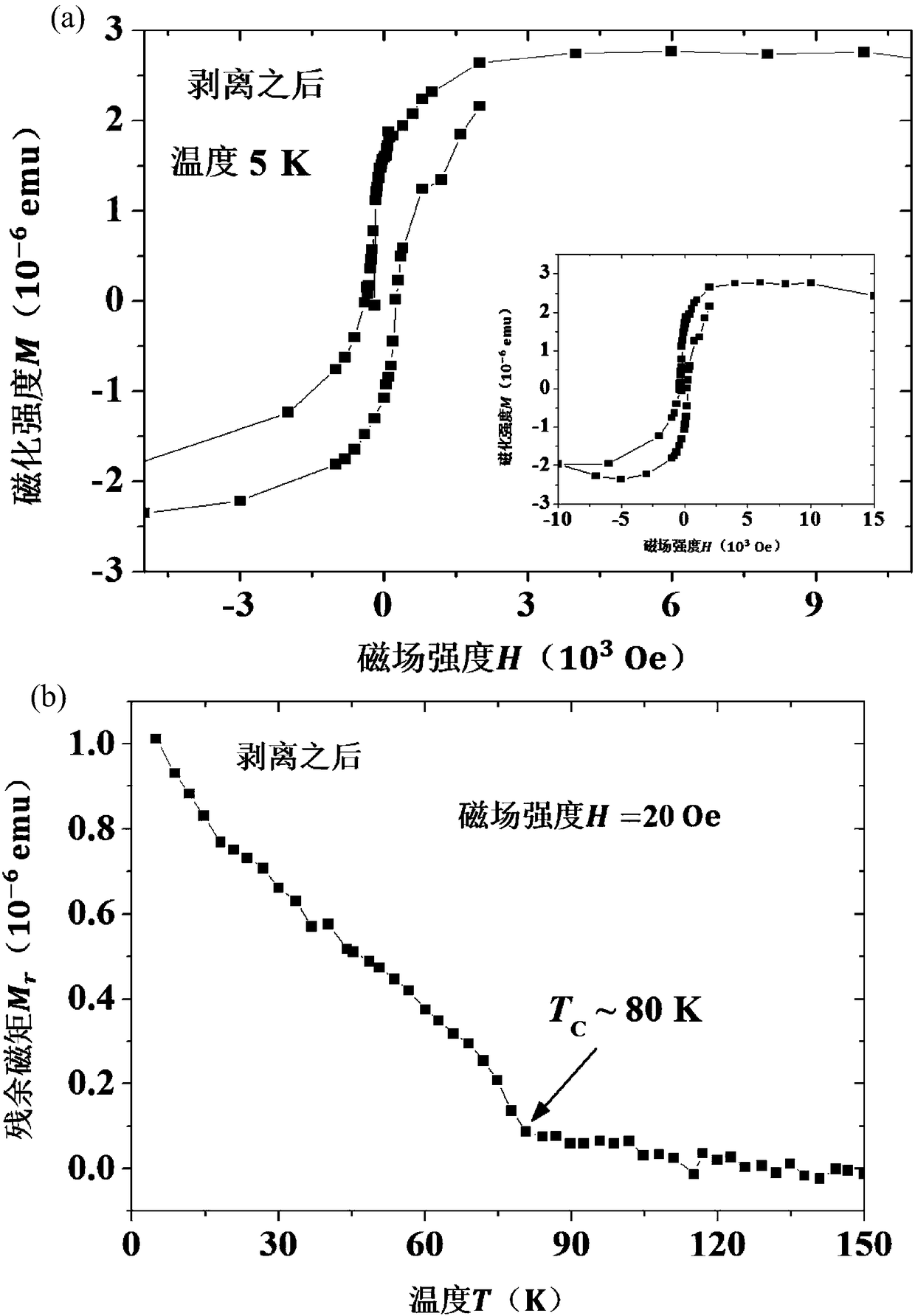
[0034] The following specific examples (Ga, Mn)As / MoS 2 The preparation method of the heterostructure and the drawings further illustrate the present invention, but do not limit the scope of the present invention in any way.

[0035] 1. Using LT-MBE technology to grow (Ga, Mn)As thin film with (Al, Ga)As sacrificial layer on GaAs substrate. The specific steps are as follows: firstly grow a 1000nm thick (Al,Ga)As sacrificial layer on the GaAs substrate by using the LT-MBE technology, with an Al content of about 80%, and then grow a 20nm thick (Ga,Mn)As.

[0036] 2. Prepare Apiezon Wax W solution for support layer. The specific steps are as follows: Dissolve 5g of Apiezon Wax W in 20mL of trichloroethylene, stir and dissolve it fully, and place it in the refrigerator for storage.

[0037] 3. Spin-coating Apiezon Wax W on the surface of the (Ga,Mn)As sample as a support. The specific steps are: cleaning the epitaxial layer sample in the order of acetone, trichloroethylene, acetone, et...


PUM

PropertyMeasurementUnit
Curie pointaaaaaaaaaa
thicknessaaaaaaaaaa

Abstract

The invention discloses a transfer method and application of a ferromagnetic semiconductor film. The method realizes transfer of a (Ga, Mn) As film on a random substrate. The transferred (Ga, Mn) As film and two-dimensional layered materials (semi-metal graphene, a semiconductor MoS2, and a superconductor NbSe2) of other different physical characteristics establish a magnetic heterostructure through a van der Waals force, and can be used for preparing novel self-spinning devices. By employing the method and application, the compatibility of the (Ga, Mn) As film with the conventional silicon process integration technology can be improved, and an important significance is attached to the application of extension of self-spinning electronics.

Description

Technical field [0001] The invention relates to the technical field of semiconductor corrosion process and thin film transfer and the field of semiconductor spintronics, in particular to a method for transferring a ferromagnetic semiconductor thin film and a method for constructing a van der Waals heterojunction using the method. Background technique [0002] The silicon-based Complementary Metal Oxide Semiconductor (CMOS) field effect transistor process has been developed to the 14nm technology node and is expected to reach its limit soon. It is necessary to find new information devices to continue Moore's Law. Spintronics, developed by controlling the degree of freedom of electron spin in semiconductors, can achieve higher density, higher speed, and lower power consumption of information storage and processing. Finding a suitable spin injection source is the key to realize semiconductor spintronics. Magnetic semiconductors have three advantages as a spin injection source: (1) ...

Claims


Application Information

Patent Timeline
Patent Type & Authority Applications(China)
IPC IPC(8): H01L43/12H01L43/10
CPCH10N50/85H10N50/01
Inventor 袁恺王海龙姚笑寒赵建华戴伦叶堉
Owner PEKING UNIV
Why Eureka
Try Eureka