Safe injector
A technology for safe syringes and injection ends, applied in the field of medical devices, can solve problems such as puncture of the side wall of the needle cap, inaccurate injection dose control, needle tip injury of patients or hospital nurses, etc., to avoid energy waste and save manpower, material and financial resources , the effect of reducing energy consumption
- Summary
- Abstract
- Description
- Claims
- Application Information
AI Technical Summary
Problems solved by technology
Method used
Image
Examples
Embodiment 1
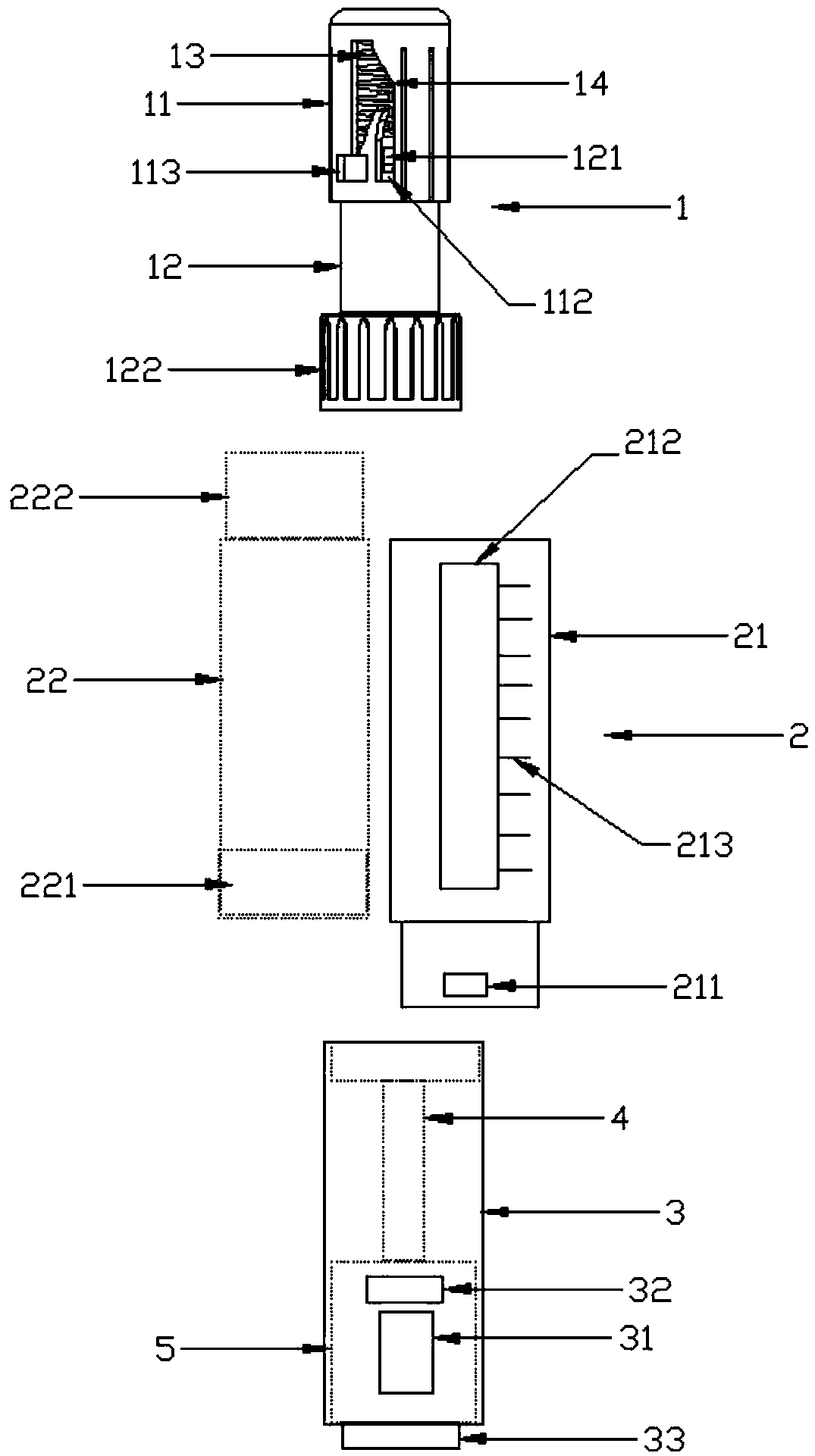
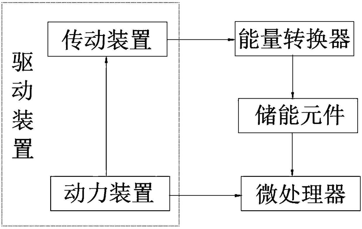
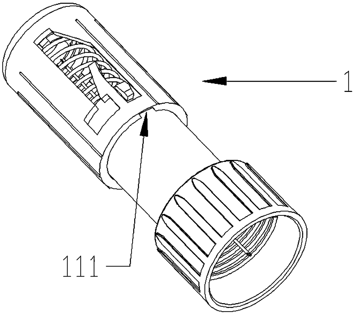
[0045] See figure 1 , figure 2 and image 3 ,
[0046] figure 1 It is a schematic structural diagram of a safety syringe in this embodiment;
[0047] figure 2 It is a structural block diagram of a safety syringe in this embodiment;
[0048] image 3 It is a perspective view of the structure of the injection end described in this embodiment.
[0049]This embodiment provides a safety syringe, which includes an injection end 1, a liquid storage device 2 and a base 3, the injection end 1 includes an injection needle 14 and a needle guard assembly, and the injection needle 14 is fixed on a needle holder 12 , the needle guard assembly includes a protective case 11 and a spring 13, one end of the spring 13 is fixedly connected to the needle hub, and the other end is fixedly connected to the protective case, and a locking structure is arranged on the protective case 11 and a first limiting groove 111, the locking structure is provided with a first locking groove 112 and a se...
Embodiment 2
[0056] See Figure 5-Figure 9 ,
[0057] Figure 5 It is a structural schematic diagram of the substrate layer described in the present invention;
[0058] Figure 6 It is a schematic structural diagram of the piezoelectric layer described in this embodiment;
[0059] Figure 7 A perspective view of the structure after the protective layer is set for the substrate layer described in this embodiment;
[0060] Figure 8 It is a schematic structural diagram of the substrate described in this embodiment;
[0061] Figure 9 It is a schematic structural diagram of the energy converter described in this embodiment.
[0062] On the basis of Embodiment 1, the energy converter includes a substrate layer 521, and the substrate layer is a crystalline silicon wafer layer, and a first opening 55 and a second opening 55 are provided on the front and back sides of the substrate layer 521, respectively. opening 56,
[0063] a second seed layer 524, the second seed layer 524 is locate...
Embodiment 3
[0080] See Figure 10 , Figure 11 and Figure 12 ;
[0081] Figure 10 It is a schematic structural diagram of the substrate described in Embodiment 3 of the present invention;
[0082] Figure 11 It is a schematic structural diagram of the interdigitated electrode described in Embodiment 3 of the present invention;
[0083] Figure 12 is a schematic structural diagram of the energy converter described in Embodiment 3 of the present invention, and Figure 12 so Figure 11 A schematic diagram of the structure viewed from top to bottom.
[0084] On the basis of Embodiment 1, the energy converter includes a substrate layer 521, and a first opening 55 and a second opening 56 are respectively provided on the front and back of the substrate layer 521,
[0085] A second conductive adhesive layer 526, the second conductive adhesive layer 526 is located at the first opening 55;
[0086] a third conductive layer 527, the third conductive layer 527 is located on the second con...
PUM
 Abstract
Description
Claims
Application Information


