
Detector for positive electron emission imaging equipment, and positive electron emission imaging equipment

A technology of positron emission and imaging equipment, applied in radiation measurement, X/γ/cosmic radiation measurement, instruments, etc., can solve problems such as poor time resolution and information loss, and achieve good time resolution and propagation time. The effect of shortening, short height

Inactive Publication Date: 2018-12-07
ZHONGPAI S&T SHENZHEN CO LTD +1
View PDF10 Cites 4 Cited by
  • Summary
  • Abstract
  • Description
  • Claims
  • Application Information

AI Technical Summary

Problems solved by technology

[0003] Compared with the latter two, detectors composed of discrete crystals do not need to use complex decoding algorithms, but due to the limitations of current technology, detectors composed of traditional discrete crystals can only decode two-dimensional position information, and the response depth direction of photons (DOI , Depth of Interaction) information is often lost, which is also a major reason that affects the imaging effect of discrete crystal detectors. At the same time, the light output and time resolution of long discrete crystals are relatively poor, and photons have to reflect many times in the crystal to reach the sensor.

Method used


Image

  • Detector for positive electron emission imaging equipment, and positive electron emission imaging equipment
  • Detector for positive electron emission imaging equipment, and positive electron emission imaging equipment
  • Detector for positive electron emission imaging equipment, and positive electron emission imaging equipment

Examples


Embodiment Construction

[0045] In the following description, numerous details are provided in order to provide a thorough understanding of the invention. However, it will be appreciated by those skilled in the art that the following description relates only to preferred embodiments of the invention and that the invention may be practiced without one or more of these details. In addition, in order to avoid confusion with the present invention, some technical features known in the art are not described.

[0046] The present invention provides a detector for a positron emission imaging device, which includes a multilayer detector module.

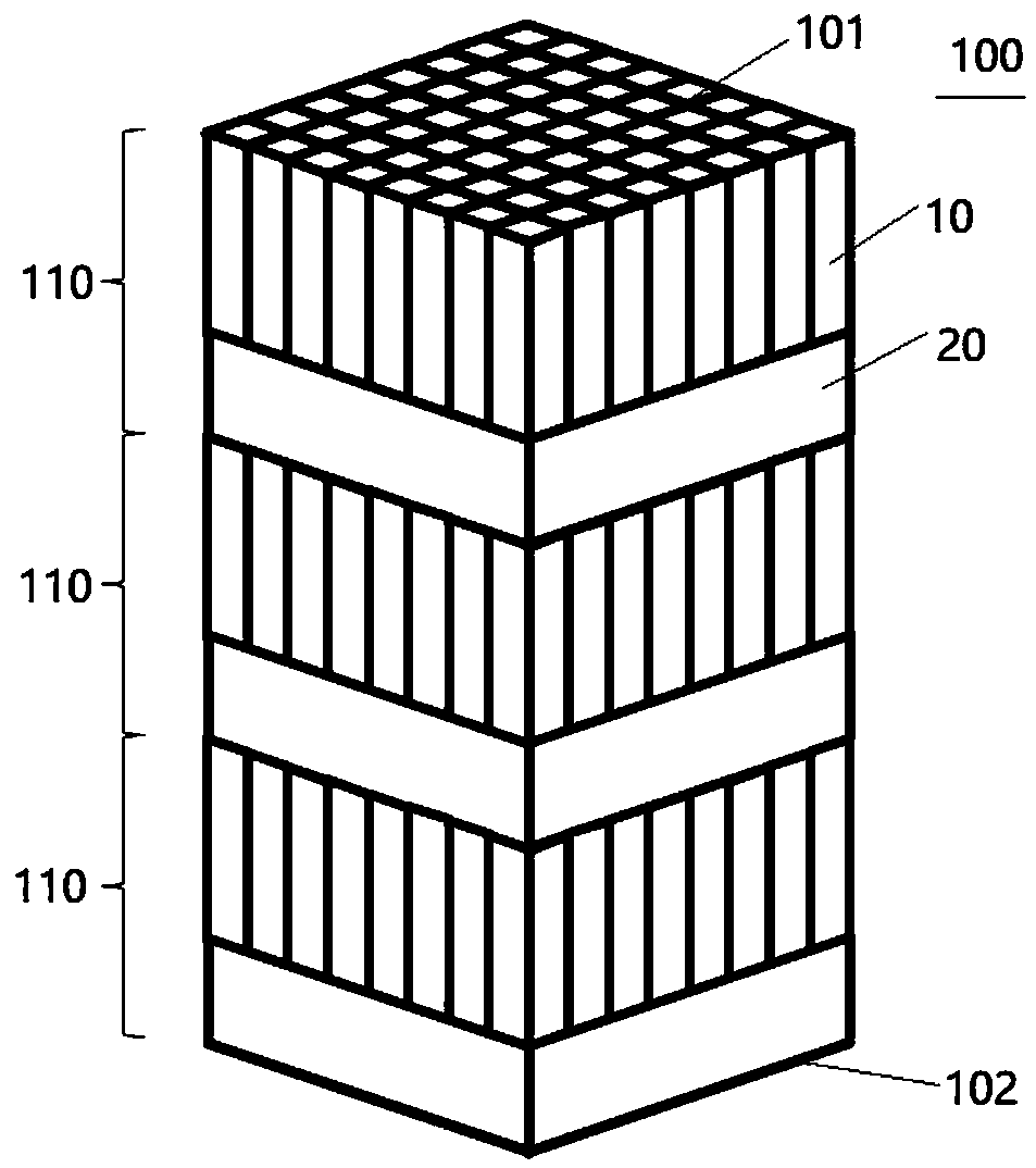
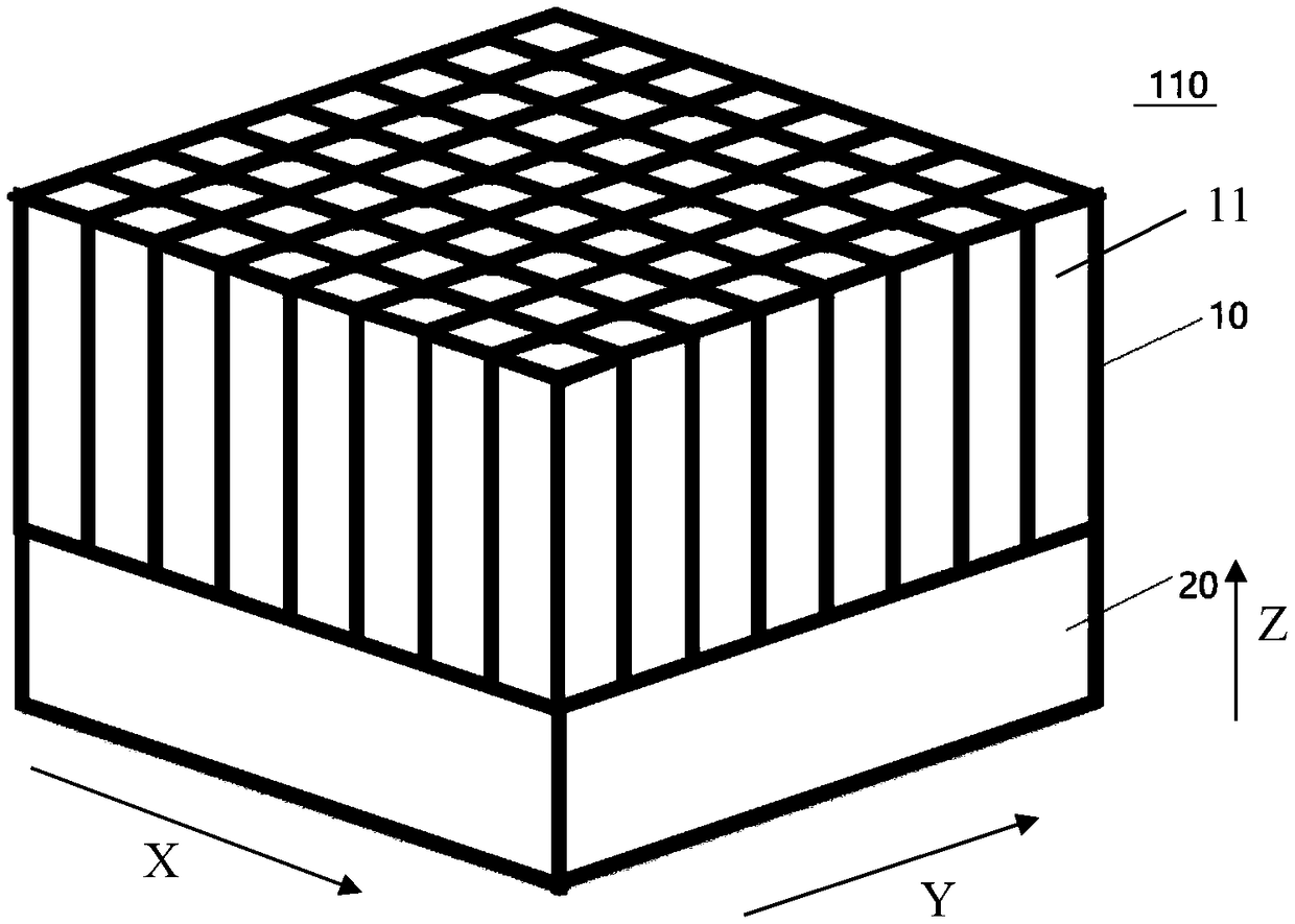
[0047] Such as figure 1 As shown, the probe 100 has an upper end surface 101 and a lower end surface 102 . The detector 100 includes multi-layer detector modules 110 arranged up and down in the height direction (although only an example of three layers is shown in the figure, in practical applications, there may be two layers, three layers, four layers, ... …), see...


PUM


Abstract

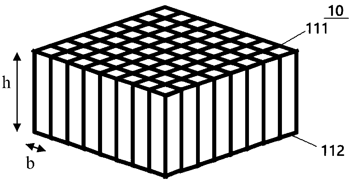
The invention provides a detector for positive electron emission imaging equipment, and positive electron emission imaging equipment. The detector is provided with an upper end surface and a lower endsurface, and includes multiple layers of detector modules arranged in a height direction up and down, wherein each layer of detector module includes a layer of scintillation crystal module and a layer of photosensor array which is coupled by a plurality of photosensors in the length and width directions; the scintillation crystal module is a scintillation crystal array coupled by a plurality of scintillation crystals in the length and width directions; the photosensor array is coupled to a lower end surface of the scintillation crystal module for detecting visible photons which are generatedduring the reaction process of light gamma photons and the scintillation crystal module; a layer of photosensor array is arranged between every two layers of scintillation crystal arrays in the multiple layers of detector modules arranged up and down; a scintillation crystal array is arranged between every two layers of photosensor arrays; and the gamma photons enters from the upper end surface, and the upper end surface is the upper surface of the scintillation crystal module located at the uppermost layer. The detector for positive electron emission imaging equipment has the advantages of high positioning capability for gamma photons, high time resolution, high sensitivity, and high spatial resolution.

Description

technical field [0001] The invention relates to the field of positron emission imaging, in particular to a detector for a positron emission imaging device and the positron emission imaging device. Background technique [0002] Positron radiation imaging is a functional imaging method because its detection principle is to detect the metabolic activity in organisms, so it is effective in the early diagnosis of major diseases such as cancer, neurological diseases, and cardiovascular and cerebrovascular diseases. At present, several detector crystals widely used in the field of positron emission tomography mainly include discrete crystal arrays, continuous crystals, and sheet crystal arrays, etc. Among them, the detectors using discrete crystals use long strip crystal arrays to interact with photoelectric converter arrays. Coupling, using methods such as the center of gravity (anger logic) or light sharing (light sharing) to realize the application of incident high-energy photon...

Claims


Application Information

Patent Timeline
IPC IPC(8): G01T1/202G01T1/29
CPCG01T1/202G01T1/2985
Inventor 解强强谢思维张熙赵指向黄秋彭旗宇
Owner ZHONGPAI S&T SHENZHEN CO LTD
Learn More